Discussion Intel current and future Lakes & Rapids thread

Page 575 - Seeking answers? Join the AnandTech community: where nearly half-a-million members share solutions and discuss the latest tech.

uzzi38

Platinum Member
Oct 16, 2019
2,565
5,575
146
2023 Macs and then the 2023 iPhone.
What makes you think either will be N3? They're skipping N3 in 2022 because of poor power/perf and density shrink relative to cost increase, especially compared to N4P. N3E is only going to be ready at the end of 2023/beginning of 2024, and so misses the production cycle for 2023 iPhone.
 

jpiniero

Lifer
Oct 1, 2010
14,510
5,159
136
What makes you think either will be N3?

They've been first at TSMC for awhile now. If N3 is really that mediocre then it makes zero sense that Intel would want it too, especially if they are dumb enough to use it for the IGP.
 

uzzi38

Platinum Member
Oct 16, 2019
2,565
5,575
146
They've been first at TSMC for awhile now. If N3 is really that mediocre then it makes zero sense that Intel would want it too, especially if they are dumb enough to use it for the IGP.
No ****?

The Meteor Lake rumour was obviously a load of bollocks right from the beginning. It's all Intel 4.

No clue about Arrow Lake, but my understanding is that's supposed to be a late 2023/2024 product, isn't it?
 

jpiniero

Lifer
Oct 1, 2010
14,510
5,159
136
No ****?

The Meteor Lake rumour was obviously a load of bollocks right from the beginning. It's all Intel 4.

Intel doesn't have the capacity to do much with Intel 4. Intel did say they were using TSMC for part of Meteor Lake but what part and what node still remains to be seen.
 

JasonLD

Senior member
Aug 22, 2017
485
445
136
What makes you think either will be N3? They're skipping N3 in 2022 because of poor power/perf and density shrink relative to cost increase, especially compared to N4P. N3E is only going to be ready at the end of 2023/beginning of 2024, and so misses the production cycle for 2023 iPhone.

Apple not using N3 in 2022 is known for a while but not in 2023 also? So noone is going to be using N3 in 2023 for the reason above? I find it hard to believe tbh lol.
 
Last edited:

mikk

Diamond Member
May 15, 2012
4,112
2,108
136
That article's sole source is this thread. Do we have any corroboration on that info?


The original source is a reddit poster called Moore's Law Is not Dead. Some of the info seems to come from the channel Moore's Law Is Dead, he talked a bit about this leak in his videos. He basically confirmed the code names, although some details/features are wrongly worded he said.


uzzi38

Platinum Member
Oct 16, 2019
2,565
5,575
146
Apple not using N3 in 2022 is known for a while but not in 2023 also? So noone is going to be using N3 is 2023 for the reason above? I find it hard to believe tbh lol.
We'll have to see I guess. Frankly speaking the base N3 is a dud, and I don't see why it sounds so strange that it might be skipped over by most companies. I'm actually hoping it is in favour of N3E and/or N4P. The latter gets you the same power/perf improvement of N3 at lower clocks, gives you an improvement at higher clocks over N5/N4 and does so at lower cost than N3.
 

repoman27

Senior member
Dec 17, 2018
342
488
136
What makes you think either will be N3? They're skipping N3 in 2022 because of poor power/perf and density shrink relative to cost increase, especially compared to N4P. N3E is only going to be ready at the end of 2023/beginning of 2024, and so misses the production cycle for 2023 iPhone.
N3 is arriving at least 3-4 months too late for the 2022 iPhone, and Apple had to know that already by Jan 2020 in order to target N4 for the A16 design. N4P was added later and won't be available until after N3. TSMC expects the first products based on N4P to tape out by the second half of 2022—which wouldn't even be in time for the 2023 iPhone. In terms of performance, TSMC's claims put N4P in the same range as N3 but at slightly higher power. Density on the other hand is 1.6x greater with N3. I don't think Apple is going to pass on that, at which point they're never going back. So I still say N3 for 2023 A-series and maybe N4P for M-series.
 

Exist50

Platinum Member
Aug 18, 2016
2,445
3,043
136
The original source is a reddit poster called Moore's Law Is not Dead. Some of the info seems to come from the channel Moore's Law Is Dead, he talked a bit about this leak in his videos. He basically confirmed the code names, although some details/features are wrongly worded he said.


The article said it wasn't by him, just an anonymous forum poster.
 

repoman27

Senior member
Dec 17, 2018
342
488
136
The original source is a reddit poster called Moore's Law Is not Dead. Some of the info seems to come from the channel Moore's Law Is Dead, he talked a bit about this leak in his videos. He basically confirmed the code names, although some details/features are wrongly worded he said.
So the original sources, MLID and AdoredTV, were allegedly incorrectly summarized by mooreslawisnotdead in a reddit comment shortly before that account was deleted. Curmudgeon666 quoted the text of that comment and linked to the subsequent discussion and reporting around it here in this thread, in what remain that user's only two posts on this forum. Right, seems totally legit.

The takeaway I got from the videos you linked to is that Arrow Lake is a mobile only / P Series version of Meteor Lake with an extra GPU tile in order to offer customers something a bit closer to Apple's IGP offerings. Their claim of up to 320 EUs would point to 2x 128 EU GPU tiles plus 64 EUs in the SoC tile. So now I'm leaning in that direction. Unless it's 2x 192 EU tiles with 64 EUs disabled, which is also a possibility, I guess.
 

jpiniero

Lifer
Oct 1, 2010
14,510
5,159
136
Intel still needs to refresh the desktop with something new in 2023. If it's not Arrow Lake then it needs to be something else, even if it's just a refresh/rebrand of Raptor Lake.

The biggest question would be what node it would be, and if it's Intel 4, where Intel would get the EUV equipment to do so.
 

mikk

Diamond Member
May 15, 2012
4,112
2,108
136
So the original sources, MLID and AdoredTV, were allegedly incorrectly summarized by mooreslawisnotdead in a reddit comment shortly before that account was deleted. Curmudgeon666 quoted the text of that comment and linked to the subsequent discussion and reporting around it here in this thread, in what remain that user's only two posts on this forum. Right, seems totally legit.

The takeaway I got from the videos you linked to is that Arrow Lake is a mobile only / P Series version of Meteor Lake with an extra GPU tile in order to offer customers something a bit closer to Apple's IGP offerings. Their claim of up to 320 EUs would point to 2x 128 EU GPU tiles plus 64 EUs in the SoC tile. So now I'm leaning in that direction. Unless it's 2x 192 EU tiles with 64 EUs disabled, which is also a possibility, I guess.


A version with 320 EUs must be for mobile of course but Arrow Lake is coming for desktop as well:


repoman27

Senior member
Dec 17, 2018
342
488
136
Intel still needs to refresh the desktop with something new in 2023. If it's not Arrow Lake then it needs to be something else, even if it's just a refresh/rebrand of Raptor Lake.

The biggest question would be what node it would be, and if it's Intel 4, where Intel would get the EUV equipment to do so.
They'll have 10% of the world's installed EUV litho equipment sitting around mostly idle at that point, so they could start there.

We'll have to see I guess. Frankly speaking the base N3 is a dud, and I don't see why it sounds so strange that it might be skipped over by most companies. I'm actually hoping it is in favour of N3E and/or N4P. The latter gets you the same power/perf improvement of N3 at lower clocks, gives you an improvement at higher clocks over N5/N4 and does so at lower cost than N3.
Is that your analysis based on what customers are saying about their test wafers / early risk starts? Or are you just spouting utter nonsense based on zero verifiable evidence?

A version with 320 EUs must be for mobile of course but Arrow Lake is coming for desktop as well:
Honestly, what makes you think there's a single shred of accurate information in those linked sources?
 

eek2121

Platinum Member
Aug 2, 2005
2,904
3,906
136
No ****?

The Meteor Lake rumour was obviously a load of bollocks right from the beginning. It's all Intel 4.

No clue about Arrow Lake, but my understanding is that's supposed to be a late 2023/2024 product, isn't it?
Apple not using N3 in 2022 is known for a while but not in 2023 also? So noone is going to be using N3 in 2023 for the reason above? I find it hard to believe tbh lol.
Well no, the last I heard, Intel is using N3, but only to supplement their Intel 4 capacity. Apple not using N3 at all is news to me. From what I understand, next year will feature a silicon refresh based on N4, then the following year on N3.
The original source is a reddit poster called Moore's Law Is not Dead. Some of the info seems to come from the channel Moore's Law Is Dead, he talked a bit about this leak in his videos. He basically confirmed the code names, although some details/features are wrongly worded he said.

Adored, MLID, and other youtubers aren't "sources". They are very poor versions of "middle-men". They take existing free content and monetize it by scouring the internet (mostly twitter) and attempting to find rumors that haven't been blasted all over. If they can't link things together, they tend to make things up. I don't believe MLID or Adored have ever been the first, or only folks to leak anything, and I know they have gotten more things wrong than right. I am not familiar with that mentioned "Moore's law is not Dead" character, but if you could link us to his profile so we can read his past posts/comments (including his deleted ones, since both public and private caches exist for reddit) it would be much appreciated.
 

jpiniero

Lifer
Oct 1, 2010
14,510
5,159
136
They'll have 10% of the world's installed EUV litho equipment sitting around mostly idle at that point, so they could start there.

I'm sure that 10% is very much not idle right now. They are using that to try to improve the yield. Yield which wasn't good enough for Aurora so it must be worse than 10 nm was during the Cannonlake fiasco.

Fabbing the Arrow Lake desktop chiplet at N3 works for me.
 
  • Like
Reactions: lightmanek

DrMrLordX

Lifer
Apr 27, 2000
21,582
10,785
136
TSMC has 3x the fab capacity of Intel. Intel will never be able to buy 100% of TSMC's capacity at the leading edge because they have neither the money nor the customers for that much silicon.

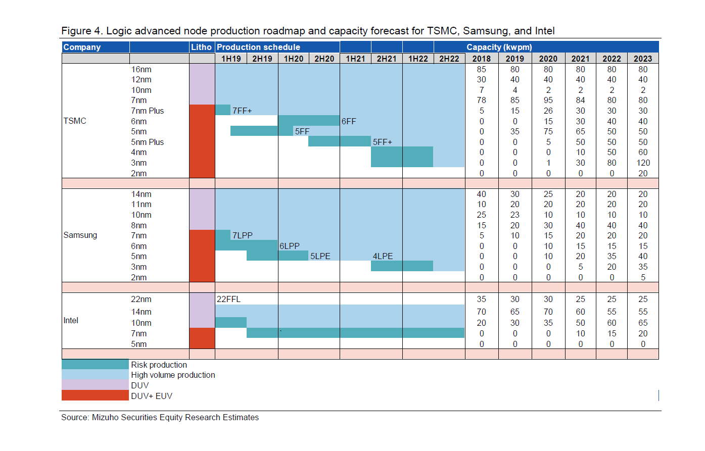
If we are to believe the Mizuho report, TSMC should have 120 kwpm of N3 alone by some point in 2023 (probably the end of the year, at this rate). That's 6x the projected wafer output of Intel 7nm/Intel 4 in the same timeframe. And (allegedly) Intel is only getting 20 kwpm of that N3 volume.

TSMC will also (allegedly) have 60 kwpm of N4 by that time. How much of that will be N4P is unknown since it isn't included in the only source I have, which is the good old Mizuho report.

Intel still needs to refresh the desktop with something new in 2023. If it's not Arrow Lake then it needs to be something else, even if it's just a refresh/rebrand of Raptor Lake.

The biggest question would be what node it would be, and if it's Intel 4, where Intel would get the EUV equipment to do so.

Arrow Lake may be a refresh of Raptor Lake on 10ESF/Intel 7. If you think about it, they will not have a lot of N3 + Intel 4 to go around! And they have to share all that between Meteor Lake, Granite Rapids, and Arc/Xe. They are also getting some N6 and N5 (apparently) so some of their products may wind up on that.

That report never once addresses whether any of TSMC's customers were underinvesting in EUV or would be more significantly impacted by supply constraints on EUV lithography equipment. TSMC may have half of all EUV systems installed to date, but that's only because they have a lot more processes using EUV doing a lot more volume than anyone else.

If TSMC has this kind of available volume, do you think that is due to them being short on EUV equipment?

E09U5KvVoAAoYZC


The dates on N3 may be pushed back a little (Q2 2022 for N3 may become Q1 2023; not really sure) but still. 120 kwpm N3? 60 kwpm N4? They're going to equal Samsung and Intel's total output for Intel 7 + Intel 4 + 4LPE + 3GAE/3GAP.
 
Last edited:
  • Like
Reactions: lightmanek

uzzi38

Platinum Member
Oct 16, 2019
2,565
5,575
146
Is that your analysis based on what customers are saying about their test wafers / early risk starts? Or are you just spouting utter nonsense based on zero verifiable evidence?

Seeing as you don't trust my word for it, apply a bit of common sense to what TSMC have publicly stated. Frankly it doesn't matter what I say in response here, does it?

Instead at TSMC's claims for wafer processing time, look at the PPA figures provided. N5 is the first instance of the increase in wafer cost drastically outstripping the increase in transistor density, N3 suffers from even worse logic, SRAM and analog shrinks than N5 had, and an even larger increase to wafer processing time.

With that you should already be able to tell that it's a dud of a node. Forget anything else I claim for now, use a bit of common sense will you?
 

mikk

Diamond Member
May 15, 2012
4,112
2,108
136
Honestly, what makes you think there's a single shred of accurate information in those linked sources?

It's from Greymon, he is one of the known trustworthy leaker on twitter. Some of them have a very good track record.

Adored, MLID, and other youtubers aren't "sources". They are very poor versions of "middle-men". They take existing free content and monetize it by scouring the internet (mostly twitter) and attempting to find rumors that haven't been blasted all over. If they can't link things together, they tend to make things up. I don't believe MLID or Adored have ever been the first, or only folks to leak anything, and I know they have gotten more things wrong than right. I am not familiar with that mentioned "Moore's law is not Dead" character, but if you could link us to his profile so we can read his past posts/comments (including his deleted ones, since both public and private caches exist for reddit) it would be much appreciated.

MLID is definitely not just a "take existing free content" user, this is just wrong. I was thinking the same long time ago but not anymore. Adored is mostly wrong I have to agree but to be fair in some rare cases he got something which is not available freely. The code name Arrow Lake was completely unknown until the reddit leak by the way and it really exists (I have a safe source for this) and Greymon confirmed it as well meanwhile which makes me think this is not just a make things up list from a random faker. The Cove and Mont names are still unknown (beside MLID, he seems to confirm them). If it turns out they are correct as well it makes the list more and more trustworthy in hindsight.
 

repoman27

Senior member
Dec 17, 2018
342
488
136
Seeing as you don't trust my word for it, apply a bit of common sense to what TSMC have publicly stated. Frankly it doesn't matter what I say in response here, does it?

Instead at TSMC's claims for wafer processing time, look at the PPA figures provided. N5 is the first instance of the increase in wafer cost drastically outstripping the increase in transistor density, N3 suffers from even worse logic, SRAM and analog shrinks than N5 had, and an even larger increase to wafer processing time.

With that you should already be able to tell that it's a dud of a node. Forget anything else I claim for now, use a bit of common sense will you?
I don't trust your word for it because you're not citing any actual numbers or public statements from TSMC, their customers, or anyone familiar with the actual performance of the node. Furthermore, what you're saying directly contradicts any credible sources that I've come across. Let's start with Anandtech's own synopsis: https://www.anandtech.com/show/16639/tsmc-update-2nm-in-development-3nm-4nm-on-track-for-2022

The only rational takeaway from that report is that when TSMC N3 reaches HVM, it will be the most advanced manufacturing process available, offering the highest transistor density, highest performance, and lowest power of any node past or present. Unless you expect the finished wafer cost to rise more than 70% over N5, then N3 will also offer the lowest transistor cost. In fact, it will almost certainly provide the lowest transistor cost in history. Are these gains less than what we might have expected historically? Absolutely—Moore's Law is running head first into the hard reality of physics.

Even if you go by the wafer costs from the CSET paper, which are almost certainly high of the mark, the increase in wafer price for N5 still did not exceed the increase in transistor density over N7. Transistor prices still went down even if they didn't decrease as much as Moore's Law would have predicted. Even as the rate of progress slows down, you're still making progress.

As for cycle times, I haven't seen anything that gives me a solid compare between nodes. The basic rule of thumb is that even though EUV steps take longer than DUV, every time you can replace a multi-patterned DUV layer with a single EUV layer, you reduce the number of steps and masks, which in turn reduces both cycle times and cost. Every time you have to add additional multi-patterning steps, you increase the number of masks, cycle times, and cost. I think N3 increases both the number of EUV layers and use of multi-patterning over N5, so we should expect longer cycle times. There's no way TSMC's wafer price will increase by 70% over N5 though, and they stuck with FinFET for N3 which should help yields and keep design costs somewhat in check.
 
  • Like
Reactions: Viknet

uzzi38

Platinum Member
Oct 16, 2019
2,565
5,575
146
I don't trust your word for it because you're not citing any actual numbers or public statements from TSMC, their customers, or anyone familiar with the actual performance of the node. Furthermore, what you're saying directly contradicts any credible sources that I've come across. Let's start with Anandtech's own synopsis: https://www.anandtech.com/show/16639/tsmc-update-2nm-in-development-3nm-4nm-on-track-for-2022

The only rational takeaway from that report is that when TSMC N3 reaches HVM, it will be the most advanced manufacturing process available, offering the highest transistor density, highest performance, and lowest power of any node past or present. Unless you expect the finished wafer cost to rise more than 70% over N5, then N3 will also offer the lowest transistor cost. In fact, it will almost certainly provide the lowest transistor cost in history. Are these gains less than what we might have expected historically? Absolutely—Moore's Law is running head first into the hard reality of physics.

Even if you go by the wafer costs from the CSET paper, which are almost certainly high of the mark, the increase in wafer price for N5 still did not exceed the increase in transistor density over N7. Transistor prices still went down even if they didn't decrease as much as Moore's Law would have predicted. Even as the rate of progress slows down, you're still making progress.

As for cycle times, I haven't seen anything that gives me a solid compare between nodes. The basic rule of thumb is that even though EUV steps take longer than DUV, every time you can replace a multi-patterned DUV layer with a single EUV layer, you reduce the number of steps and masks, which in turn reduces both cycle times and cost. Every time you have to add additional multi-patterning steps, you increase the number of masks, cycle times, and cost. I think N3 increases both the number of EUV layers and use of multi-patterning over N5, so we should expect longer cycle times. There's no way TSMC's wafer price will increase by 70% over N5 though, and they stuck with FinFET for N3 which should help yields and keep design costs somewhat in check.
Their 7nm cost per wafer is significantly overvalued.

5nm isn't bad though. More likely than not it's just by chance though. Fact of the matter is that cost per transistor has been rising since 16/14nm nodes.

Also, you're being extremely generous by claiming it needs to be 70% higher cost per wafer to be a worse deal, as you're disregarding the poor SRAM scaling (1.2x) and analog scaling (1.1x) of N3. Look at A14 vs A13, only a 35% improvement to overall transistor density despite technically being a better shrink (1.8x logic, 1.35x SRAM can't remember analog logic), with N3 you'd see even less than that, more likely only a 20-25% improvement to transistor density at best.
 
  • Like
Reactions: Tlh97