I noticed that the versions of the Meteor Lake package rendering that are currently publicly available from Intel all appear to have somewhat redacted labels on the top tiles. The slide I posted previously shows the following labels:
CPU Tile
SOC Tile
GPU Tile
All of which are very generic and use the Intel preferred terminology of "tile" rather than "die" or "chiplet". Slides and screenshots posted by media outlets the day of the Intel Accelerated presentation showed slightly different labels for those tiles. According to the timestamp,
VideoCardz posted this version of the slide slightly before the embargo lifted:
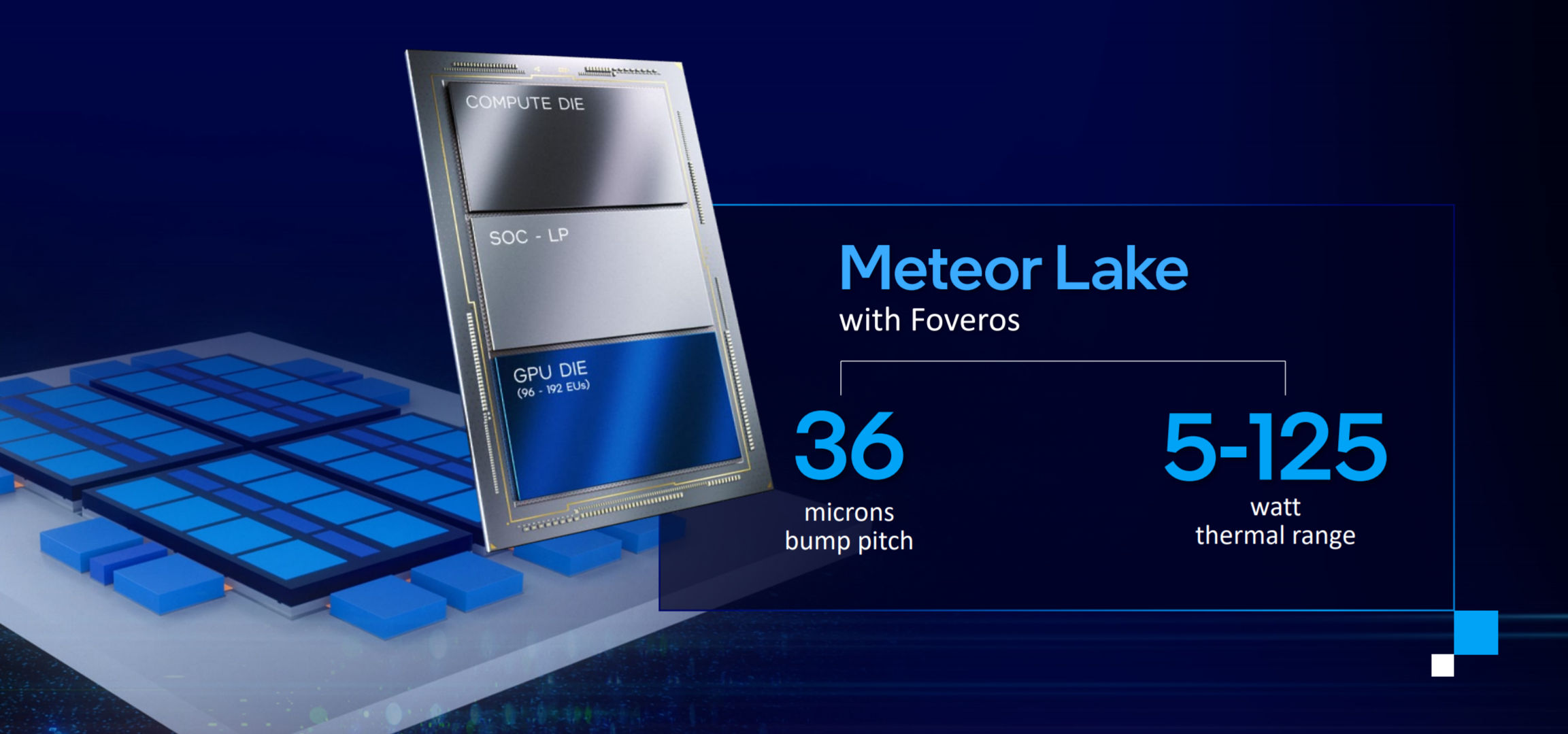
Here we see the tiles labeled as:
COMPUTE DIE
SOC - LP
GPU DIE (96 - 192 EUs)
"SOC - LP" would seem to indicate that this is a mobile variant, and that there is probably a corresponding "SOC - HP" for desktop processors. Compute and GPU are referred to as dies rather than tiles, and that may point to their nature as having been disaggregated from the SoC proper. The GPU die includes a range of EU counts. Seeing as this is a mobile processor, as indicated by the "SOC - LP", that range might only be applicable to the GT2 version of the GPU. Perhaps this is a bit of unintended disclosure by Intel, or simply reuse of an image that was designed to more specifically represent the mobile CPU package. At first I thought it might have been due to VideoCardz jumping the gun with some unofficial leaked slides, but
WikiChip posted what appears to be a frame capture from the live webcast that included the same image:
Although this package rendering is highly stylized and not to scale, I do believe it may accurately represent the three active top tiles and their relative positioning in regards to MTL-M/P.
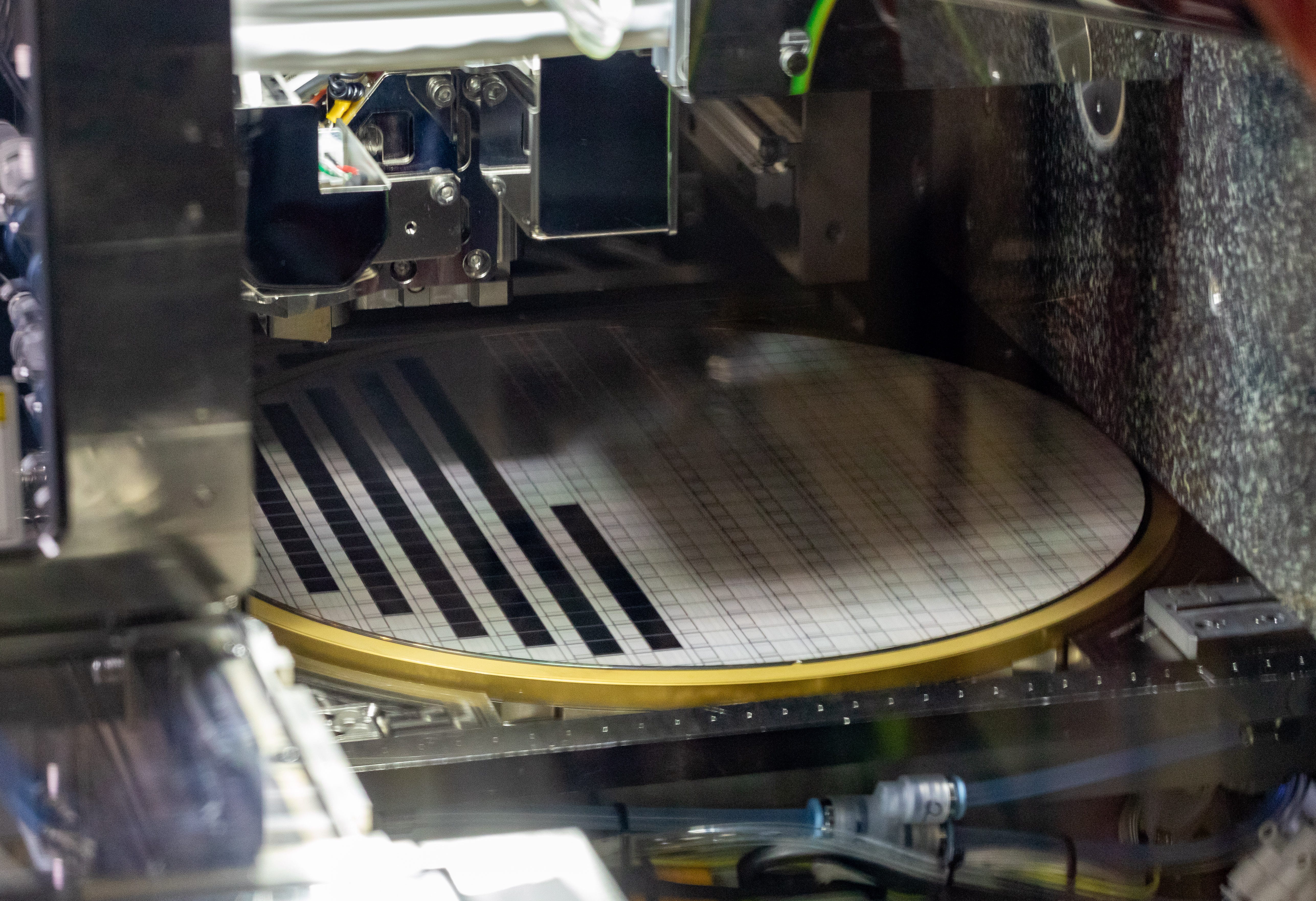
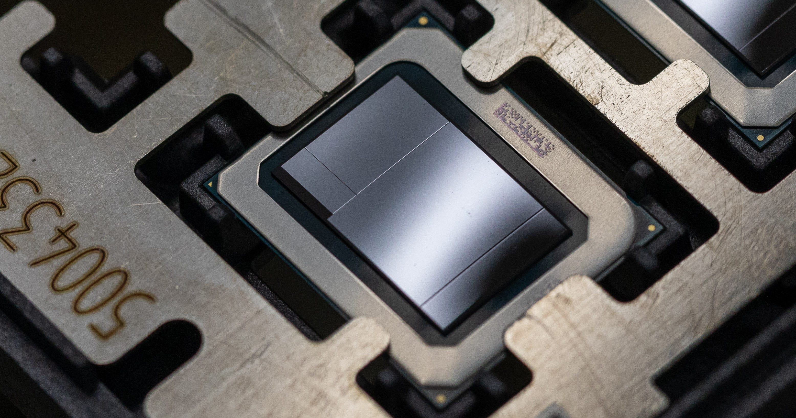
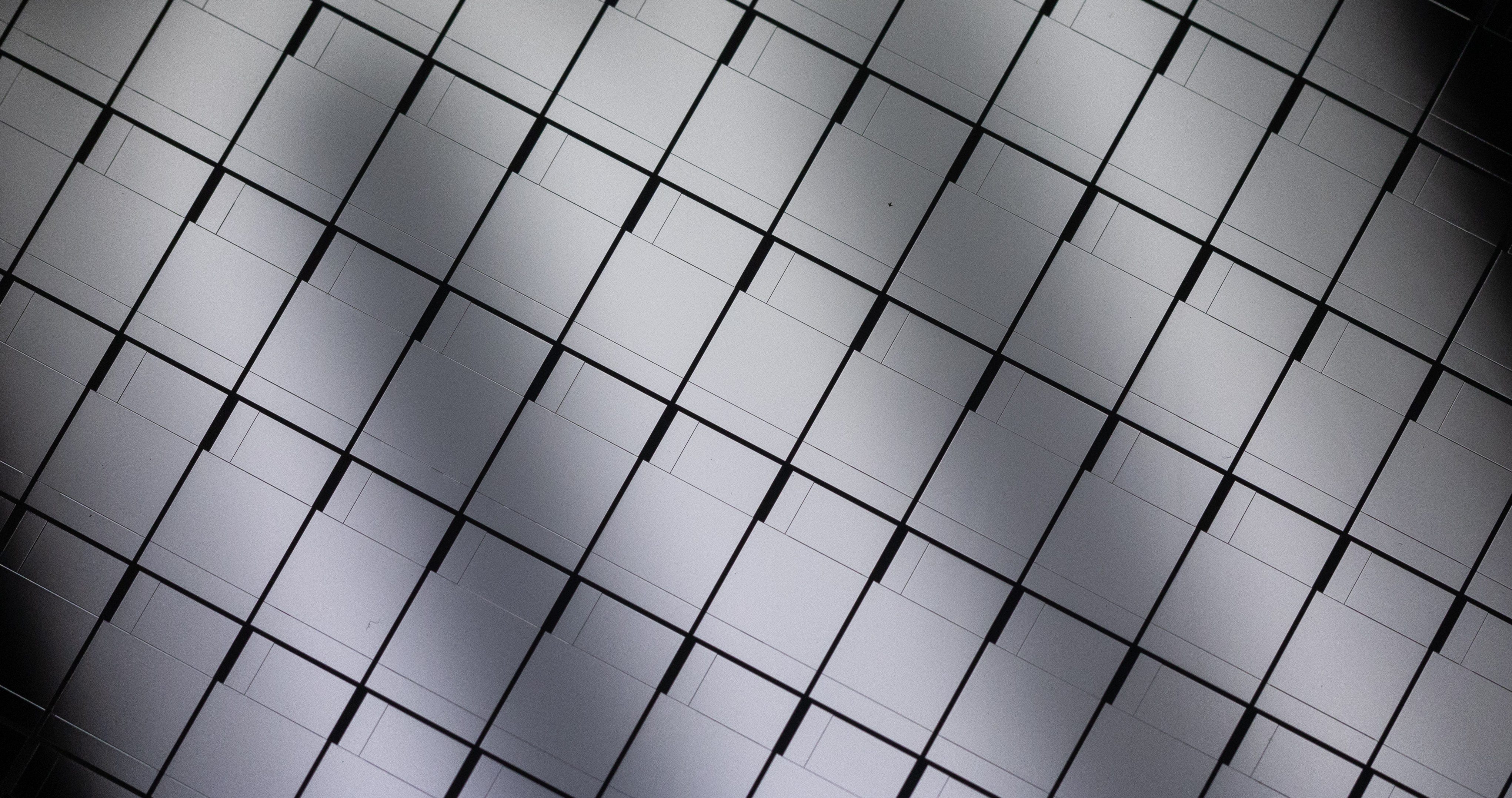
Taking the top tiles in turn, Intel has disclosed that the Meteor Lake CPU tile is being manufactured using the Intel 4 process and they even showed off a test wafer. Based on that, I calculated the die size to be 4.8 mm x 7.9 mm = 37.92 mm². I also made my own measurements of the CPU area of the ADL 8+8+1 HP die based on
a high-resolution die shot and came up with 111.28 mm². Lopping off 4 Golden Cove performance cores to get a theoretical 4+8 configuration, which is what I think I'm seeing on the Meteor Lake CPU test wafer, yields an area of 69.11 mm². If we assume 2x density scaling for Intel 4 over Intel 7, that would shrink it down to 34.56 mm², which is a pretty good fit. Although we would expect Redwood Cove and Crestmont (if those code names are indeed correct) to be a bit fatter than Golden Cove and Gracemont, if the L3$ moved to the base tile, there would still be plenty of room for the cores to grow. MTL-P could ditch the little structural tile and use a longer 6+8 CPU tile. MTL-S would probably switch to a different base tile and SoC-HP tile and possibly use two of the 4+8 CPU tiles for an 8+16 configuration.
Despite what many folks are saying, the largest of the top tiles, the one in the middle, is the SoC tile. I measured that tile using the CNET photos and came up with 9.0 mm x 10.5 mm = 94.5 mm². If we take the ADL 8+8+1 HP die as an example and subtract the CPU and GPU areas, we get 209.1 - 111.28 - 12.31 = 85.51 mm² for "everything else", a.k.a. "SoC". And that's not including the sizable IPU and Thunderbolt 4 blocks typically present on mobile processors. So 94.5 mm² on Intel 7 might actually be cutting it rather fine. However,
a recent report from the Taiwan based Commercial Times claims that not only will the GPU tile for Meteor Lake be manufactured on TSMC N3, but the SoC tile will be made using TSMC N5 or N4. Although this seems bonkers to me, it would give Intel a density increase of 1.66x or 1.76x respectively over using Intel 7 and probably offer considerable power savings to boot. This may even be necessary due to additional area requirements resulting from disaggregation. In keeping with historical precedent, it's also possible that the SoC-HP tile will forgo integrated Thunderbolt and IPU and instead include a 64 EU GT1 GPU, obviating the requirement for a separate GPU tile.
Finally, the long skinny tile is the GPU tile, housing 192 Gen12 EUs manufactured on TSMC N3. My measurements of this tile based on the CNET photos came in at a troublingly small 2.25 mm x 10.5 mm = 23.625 mm². Going back to the ADL 8+8+1 HP die and measuring the 32 EU GT1 slice, I came up with an area of 12.31 mm². However, I realized that a more apt comparison is the 96 EU GT2 GPU from the TGL 4+2 LP die, which is still Gen12 but uses a denser layout to achieve an area of just 32.72 mm² on 10nm SuperFin. Doubling the number of EUs on TSMC N3 which offers 2.83x density would result in an area of 23.12 mm². That would just barely fit given my die measurements, but would have some room to breathe if Locuza's estimate of 2.6 mm x 11.0 mm = 28.6 mm² turns out to be closer to the actual dimensions. One final possibility is that the SoC-LP tile includes 64 EUs and the GPU tile is simply an additional 128 EU slice used for GT2 configurations, although that strikes me as unlikely.


 . I think ADL-P has a good chance at beating Cezanne though once you get down to the 45W range or so and lower.