Discussion Intel current and future Lakes & Rapids thread

Page 572 - Seeking answers? Join the AnandTech community: where nearly half-a-million members share solutions and discuss the latest tech.

jpiniero

Lifer
Oct 1, 2010
16,132
6,594
136
I thought about the big tile being SoC but Intel also said they were using Foveros. Figured they would be doing the same thing they did with Lakefield and that the SoC is the base tile.

If it is the SoC I would say it would have to have a bunch of other stuff like the L3.
 

repoman27

Senior member
Dec 17, 2018
384
540
136
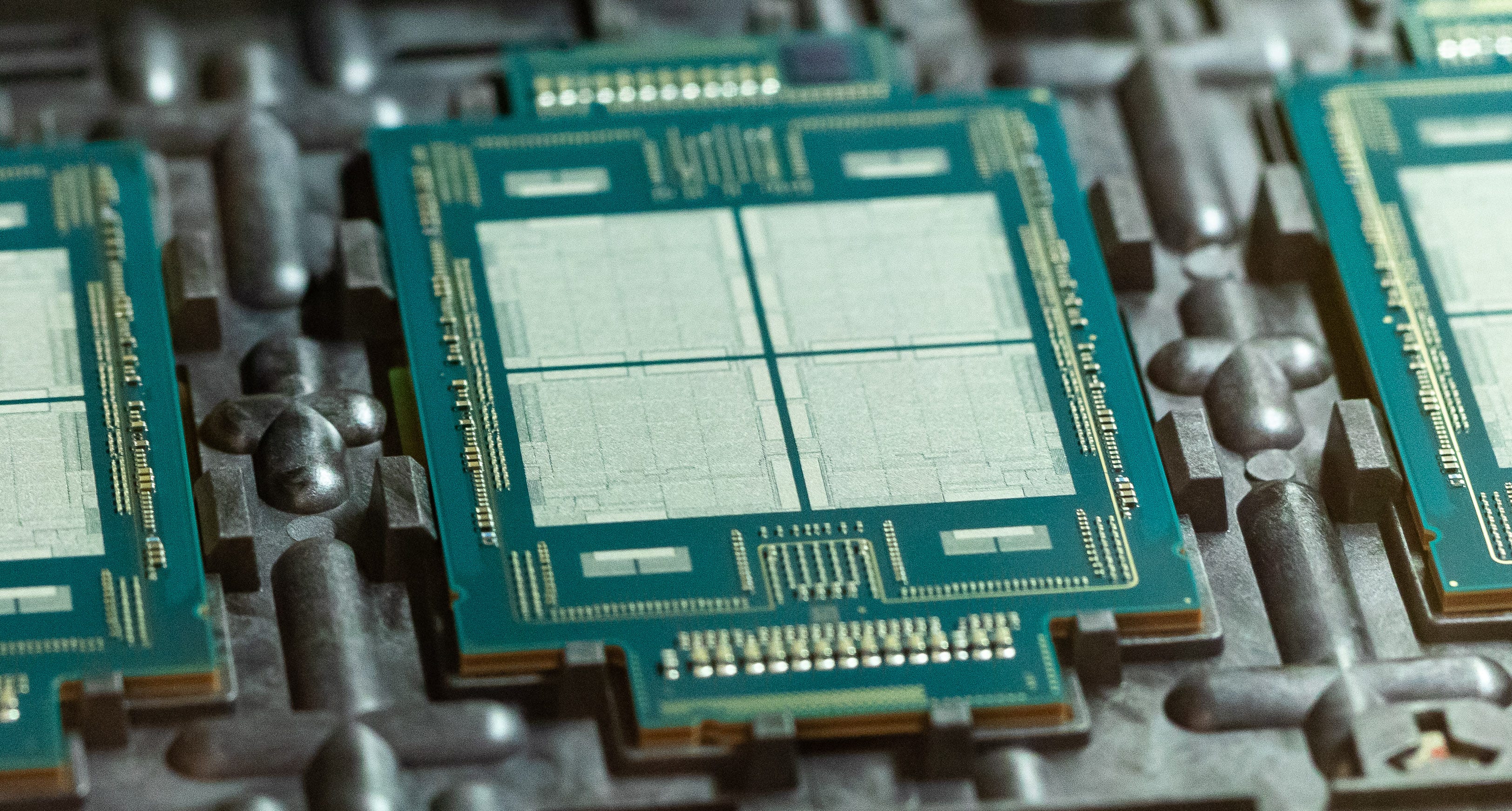
My measurements of the MTL client compute tile based on the wafer shots provided by Intel during the Intel Accelerated event are 4.85 mm x 8 mm = 38.8 mm², which checks out against Locuza's estimates. Pretty sure the larger center tile is actually the "SOC-LP" (despite being a total misnomer, that's the terminology Intel is using). It's huge because it's Intel 7 (née 10+++ / 10ESF) vs. Intel 4 (née 7nm), which is what the compute tile is made on. The skinny tile on the left is the GPU tile, which is comparatively tiny because it's TSMC N3. The little tile above the CPU die might be cache.

edit: The Foveros base die is probably the PCH, on either Intel 7 or good ol' 14nm. This would appear to be a single chip / mobile platform.
 
Last edited:

repoman27

Senior member
Dec 17, 2018
384
540
136
I disagree. We have seen only one EMIB chiplet at the edge in all the previous Intel implementations (e.g. See Ponte Vecchio). SPR will come with different chiplet sizes; Intel says UPTO ~400mm2 Per chiplet. SPR with HBM will likely come with two different SPR tile sizes as well, or at least it’s planned as a “backup” based on what AMD does. It could also just be for Aurora. Clearly it has been planned that way. We can agree to disagree and wait for Q1/Q2 next year.
Jeezy Pete, that CNET article has amazing photos of the SPR substrate in both unpopulated and populated states. The SPR XCC compute tiles are 426.4 mm². There are two because there is a left and right that have floor plans that are essentially mirror images, but they are the same dimensions. The only tile between the compute tiles and the HBM2E stacks is the EMIB, which is embedded in the organic substrate.

edit: The green solder mask covers the top layer of the PCB and EMIB dies, but there's only a single EMIB die linking each compute tile to its HBM stack, and five EMIB dies linking each compute tile to its neighbors.

20210819-intel-arizona-fab-02.jpg

20210819-intel-arizona-fab-05.jpg
 
Last edited:

mikk

Diamond Member
May 15, 2012
4,287
2,370
136
Pick One. Arrow Lake is mobile only, or Meteor Lake is. Not both I don’t claim to have amazing sources, but hint: Intel is on a slightly-less-than-yearly cadence with desktop. Intel is currently following a tick tock with desktop/mobile. Big changes are mobile first.


Arrow Lake is the real Raptor Lake-S successor most likely, of course we cannot rule out a limited Broadwell (edram) launch for desktop. Broadwell mobile launched 8 months before Skylake DT. Meteor Lake two quarters before Arrow Lake looks suspiciously similar from the timeline.
 

repoman27

Senior member
Dec 17, 2018
384
540
136
The retail on a whole spool of Sapphire Rapids chiplets must be pretty dang expensive... Probably has a few hundred chiplets on one spool.
To Intel, those are cheap and made in house. The price tag on that spool of 16GB HBM2E MKGDS is what I was pondering...
 

dullard

Elite Member
May 21, 2001
25,765
4,292
126
Also, that's definitely 2+8.
I'm wondering what I'm doing wrong with my calculations then. Based off of this Alder Lake image https://i.redd.it/lyhmdzo6c3w71.jpg the P core is ~9.8 mm^2 (including core, cache, FPU). Based off that same image, the 4 E core cluster is ~12.9 mm^2 (including 4 cores, cache). So, an Alder Lake 2+8 would be roughly 45.4 mm^2. I just don't see the Meteor Lake 2+8 being just about that same area given that it is on Intel 4.
 
  • Like
Reactions: mikk

vstar

Member
May 8, 2019
46
39
61
I'm wondering what I'm doing wrong with my calculations then. Based off of this Alder Lake image https://i.redd.it/lyhmdzo6c3w71.jpg the P core is ~9.8 mm^2 (including core, cache, FPU). Based off that same image, the 4 E core cluster is ~12.9 mm^2 (including 4 cores, cache). So, an Alder Lake 2+8 would be roughly 45.4 mm^2. I just don't see the Meteor Lake 2+8 being just about that same area given that it is on Intel 4.

There was also this rumor that the MTL compute die is in a 6P+8E configuration, so that might explain things.


dullard

Elite Member
May 21, 2001
25,765
4,292
126
There was also this rumor that the MTL compute die is in a 6P+8E configuration, so that might explain things.

Maybe. But then Intel 4 must be quite dense to fit 6P+8E into the 2nd largest tile. 4P+8E seems much more likely for a ~40 mm^2 area on Intel 4. I have no answers, but a 2P+8E Intel 4 in ~40 mm^2 just doesn't fit the sniff test unless cache or something else really huge is added.
 
Last edited:
  • Like
Reactions: mikk

jpiniero

Lifer
Oct 1, 2010
16,132
6,594
136
Arrow Lake is the real Raptor Lake-S successor most likely, of course we cannot rule out a limited Broadwell (edram) launch for desktop.

No need. I figure if there is any really leaky stuff left they will just dump it on AIO BGA desktops like they've done with Tiger Lake.

The skinny tile on the left is the GPU tile, which is comparatively tiny because it's TSMC N3.

The IGP is not important enough to use N3. It'd have to be dual sourcing the CPU tile. Still assuming that they are either giving Raptor Lake mobile a full release (and it's going to be like Comet/Ice) or the CPU tile needs to be dual sourced.
 

Saylick

Diamond Member
Sep 10, 2012
3,882
9,016
136
To Intel, those are cheap and made in house. The price tag on that spool of 16GB HBM2E MKGDS is what I was pondering...
Right, but that's why I said "retail price". ;) While it costs Intel probably like $100 to fab each 400mm2 chiplet, the MSRP on a complete SPR chip, sans HBM, is in the thousands of dollars.
 

TESKATLIPOKA

Platinum Member
May 1, 2020
2,696
3,259
136
Maybe. But then Intel 4 must be quite dense to fit 6P+8E into the 2nd largest tile. 4P+8E seems much more likely for a ~40 mm^2 area on Intel 4. I have no answers, but a 2P+8E Intel 4 in ~40 mm^2 just doesn't fit the sniff test unless cache or something else really huge is added.
MTL will have new P-core and E-core, so they should be bigger than the cores in ADL, If they were made using the same process. More cache is also very likely.
If Intel 4 is 1.8-2x denser than Intel 7 then this wouldn't explain the size, so more cores is a very likely and in that case I am also voting for 4P+8E.
 

Ajay

Lifer
Jan 8, 2001
16,094
8,111
136
MTL will have new P-core and E-core, so they should be bigger than the cores in ADL, If they were made using the same process. More cache is also very likely.
If Intel 4 is 1.8-2x denser than Intel 7 then this wouldn't explain the size, so more cores is a very likely and in that case I am also voting for 4P+8E.

4P+8E would indicate another process failure on Intel's part.
 
Last edited:

TESKATLIPOKA

Platinum Member
May 1, 2020
2,696
3,259
136
4P+8P would indicate another process failure on Intel's part.
Why? Because It is only 4P+8E?
4P+8E ADL would be 4*9.8mm^2 + 2*12.9 mm^2 = 65mm^2 on Intel 7.
Add to It more cache and faster(bigger) cores, I don't see why It couldn't be 72-80mm^2 on Intel 7, which would translate to ~40mm^2 using Intel 4 process, If It is ~1.8-2x denser.
 

repoman27

Senior member
Dec 17, 2018
384
540
136
The IGP is not important enough to use N3. It'd have to be dual sourcing the CPU tile. Still assuming that they are either giving Raptor Lake mobile a full release (and it's going to be like Comet/Ice) or the CPU tile needs to be dual sourced.
What? The IGP for their most important client Client platform isn't important enough to use N3 for? Why? Why would you possibly outsource that product and not use the best manufacturing node available to you? Why do you think Intel is rumored to be the lead customer for TSMC N3?

And there is literally zero chance that Intel would dual-source the compute tile, which would be almost impossible to do with a Foveros design anyway. They can fit something like 1600 of those tiles on a single wafer (I didn't have patience to count them to get the exact number), but even if every Intel laptop sold in 2023 had Meteor Lake inside, they would only need ~8K WSPM on Intel 4.
 
  • Like
Reactions: mikk

jpiniero

Lifer
Oct 1, 2010
16,132
6,594
136
What? The IGP for their most important client Client platform isn't important enough to use N3 for? Why? Why would you possibly outsource that product and not use the best manufacturing node available to you?

The IGP is important but it's not spend a billion dollars a quarter at TSMC important.

Why do you think Intel is rumored to be the lead customer for TSMC N3?

but even if every Intel laptop sold in 2023 had Meteor Lake inside, they would only need ~8K WSPM on Intel 4.

You're assuming Intel 4 yields aren't garbage. That's why they would need something else.
 

repoman27

Senior member
Dec 17, 2018
384
540
136
The IGP is important but it's not spend a billion dollars a quarter at TSMC important.
Judging by the die area dedicated to it, It's the most important part of a GT2 chip. And compared to the tens of billions of dollars Intel is spending on their own fabs, which won't even get them close to TSMC N3 capabilities by Q1'23, I'd say it actually has the potential to improve Intel's margins.
 

repoman27

Senior member
Dec 17, 2018
384
540
136
Why? Because It is only 4P+8E?
4P+8E ADL would be 4*9.8mm^2 + 2*12.9 mm^2 = 65mm^2 on Intel 7.
Add to It more cache and faster(bigger) cores, I don't see why It couldn't be 72-80mm^2 on Intel 7, which would translate to ~40mm^2 using Intel 4 process, If It is ~1.8-2x denser.
I assumed that the compute tile would be at least 6+8 to maintain parity with ADL-P, but I think you could be right. The more I look at this wafer shot, the more I think it is 4P+8E:

MTL-wafer.jpg
 

jpiniero

Lifer
Oct 1, 2010
16,132
6,594
136
Judging by the die area dedicated to it, It's the most important part of a GT2 chip.

The alternative really is Intel 7. Which if they have the capacity is basically free. Not from an accounting perspective from a cash spending one.

A good chunk of the IGP is the fixed function which could be on any node I reckon.
 

repoman27

Senior member
Dec 17, 2018
384
540
136
The alternative really is Intel 7. Which if they have the capacity is basically free. Not from an accounting perspective from a cash spending one.

A good chunk of the IGP is the fixed function which could be on any node I reckon.
192 EUs on Intel 7 is not free from an area or power perspective though. Customers, by which I mean OEMs, would definitely balk at that.

And yeah, I was wondering how much of the media encoding blocks and whatnot will be located in the SOC-LP die, which probably will be Intel 7.
 
  • Like
Reactions: mikk

Exist50

Platinum Member
Aug 18, 2016
2,452
3,105
136
I'm wondering what I'm doing wrong with my calculations then. Based off of this Alder Lake image https://i.redd.it/lyhmdzo6c3w71.jpg the P core is ~9.8 mm^2 (including core, cache, FPU). Based off that same image, the 4 E core cluster is ~12.9 mm^2 (including 4 cores, cache). So, an Alder Lake 2+8 would be roughly 45.4 mm^2. I just don't see the Meteor Lake 2+8 being just about that same area given that it is on Intel 4.

What assumptions are you making for density? CPU core and CCF scaling isn't likely to be ideal. That aside, new gen (barely), bigger chips, and there're also globals/die2die overhead to consider.

There was also this rumor that the MTL compute die is in a 6P+8E configuration, so that might explain things.


A 6+8 die exists, but that clearly ain't it. Another problem there is assuming any active logic in the base die.
 

DrMrLordX

Lifer
Apr 27, 2000
22,540
12,405
136
The alternative really is Intel 7. Which if they have the capacity is basically free. Not from an accounting perspective from a cash spending one.

A good chunk of the IGP is the fixed function which could be on any node I reckon.

Isn't that was the whole point of the tiled approach anyway? Intel is only going to have so much 7nm/Intel 4 to go around, so they need to be careful on how they "spend" it. Granite Rapids will be an area-hungry beast, and we have no idea how much Intel's other projects will consume their N3 allocation. Surely most N3 will go to some Arc variant, assuming they don't kill Arc entirely.
 

naukkis

Golden Member
Jun 5, 2002
1,004
844
136
What? The IGP for their most important client Client platform isn't important enough to use N3 for? Why? Why would you possibly outsource that product and not use the best manufacturing node available to you? Why do you think Intel is rumored to be the lead customer for TSMC N3?

Because IGP can be scaled to older processes just fine. Double the EU units on older process will be competitive with every aspect of half the EU's on newer process. TSMC N3 will be extremely expensive and low output node for Intel, they as they said will be using it to their halo products not for IGP for mainstream parts.
 

repoman27

Senior member
Dec 17, 2018
384
540
136
OK, let's do the math here.

Given a 2.6 mm x 11.0 mm die, you can obtain 2177 dies per 300 mm wafer. If TSMC N3 defect densities follow the trend established by N7 and N5, we would expect around 0.11 defects per cm² at the beginning of the HVM ramp. Using the Seeds model, a 28.6 mm² die would see a yield rate of 96.95%, or 2110 fully functional dies per wafer. At a cost of $20,500 per finished wafer, each GPU die would cost Intel $9.72.

Just the GPU slice (not including media block or display engine) for ADL 8+8+1 is 16.64 mm². That's for 32 EUs on Intel 7, so 192 Gen12 EUs would work out to ~100 mm². You can fit 626 9.0 mm x 11.0 mm dies on a 300 mm wafer. A 99 mm² die and a D0 of 0.10 would result in a 90.99% yield rate, or 569 fully functional dies per wafer. A finished Intel 7 wafer would have to cost $5,500 or less to compete with TSMC N3.

Notebook PC platforms are Intel's iPhone. They generate more revenue and profit for Intel than any other product they produce. Intel currently has locked in customers for ~130 million U Series chips with IGPs annually vs. 0 for desktop discrete GPUs. A best case scenario for Intel would be reaching something like 8 million dGPUs in 2023. The first Arc products, slated to ship in Q1'22, are based on the Alchemist GPU which is being manufactured on TSMC N6. It is incredibly unlikely that the follow up, Battlemage, will be a Q1'23 product made entirely on TSMC N3. However, a 192 EU tile at just 28.6 mm² that could be used for both IGPs and dGPUs is a perfect lead-off product on a new manufacturing node.
 
  • Like
Reactions: moinmoin