Question Zen 6 Speculation Thread

Page 275 - Seeking answers? Join the AnandTech community: where nearly half-a-million members share solutions and discuss the latest tech.

OneEng2

Senior member
Sep 19, 2022
878
1,130
106
Can't believe this needs to be stated, but why on earth are you comparing CCD area (meaning, only cores + IFOP) and the whole SoC, that has the CPU cores, the NPU, memory controllers and a relatively big iGPU? This is not an apples-to-apples comparison.
To the best of my understanding, the whole SoC is quite large. A single CCD is quite small. Don't look at it as the cumulation of CCD's is X mm2. Look at it as "I can get X number of good products from Y number of wafers" and "Total cost of one big SoC is X and Total cost of chiplets to do the same thing is Y".

Chiplets have proven to be a superior method of achieving the most value per $. Monolithic designs have proven to be superior in overall performance.

Chiplets also offer design modularity at a level beyond what can be reached with monolithic designs.

So my point is that should AMD desire to match the performance of M5 with Zen 6, and cost wasn't a factor, and modularity wasn't a factor, and scalability wasn't a factor, they could do it, but the design would be quite different than the Zen 6 we will be getting.

So it is an Apples to Apples comparison. Zen 6 is a more saleable design in both number of cores AND performance per $ (and likely design effort efficiency across a broad range of products).

If AMD's Zen 6 design targets were the same as M4, I am certain Zen 6 would look much more like M4.
 

poke01

Diamond Member
Mar 8, 2022
4,347
5,664
106
To the best of my understanding, the whole SoC is quite large. A single CCD is quite small. Don't look at it as the cumulation of CCD's is X mm2. Look at it as "I can get X number of good products from Y number of wafers" and "Total cost of one big SoC is X and Total cost of chiplets to do the same thing is Y".

Chiplets have proven to be a superior method of achieving the most value per $. Monolithic designs have proven to be superior in overall performance.

Chiplets also offer design modularity at a level beyond what can be reached with monolithic designs.

So my point is that should AMD desire to match the performance of M5 with Zen 6, and cost wasn't a factor, and modularity wasn't a factor, and scalability wasn't a factor, they could do it, but the design would be quite different than the Zen 6 we will be getting.

So it is an Apples to Apples comparison. Zen 6 is a more saleable design in both number of cores AND performance per $ (and likely design effort efficiency across a broad range of products).

If AMD's Zen 6 design targets were the same as M4, I am certain Zen 6 would look much more like M4.
You do know the most comparable product to M4 that AMD makes is Strix Point, a monolithic laptop SoC?
 

OneEng2

Senior member
Sep 19, 2022
878
1,130
106
You do know the most comparable product to M4 that AMD makes is Strix Point, a monolithic laptop SoC?
Good point.

232.5 mm2; however, its performance is not as good as Strix Halo which is a chiplet design.

Still, if you look at the performance per $, I wonder how this pans out?
 

Tigerick

Senior member
Apr 1, 2022
866
804
106
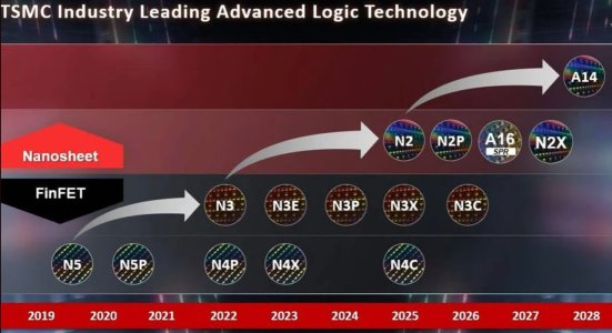
Geez, sometimes the roadmap is so stupid and yet people still believe Zen6 12-core CCD will be fabbed by N2P/N2X....

TSMC.jpg

Let me repeat: Venice is 32-core CCD fabbed by N2; not N2P or N2X. Meanwhile 12-core Zen6 will be fabbed by N3P/N3X. I am more inclined to believe it's N3X, same as Zen5 CCD, N4X. The rest of Zen 6 APUs and Soundwave will be fabbed by N3P. And it is aligned with TSMC's roadmap. That' why it is funny MLID speculated Zen6 will be delayed based on AMD roadmap; even though TSMC roadmap shown something more believable. :rolleyes:
 
Last edited:

ETI4711

Junior Member
Oct 25, 2025
2
4
36

Q: By the way, CEO Lisa Su has already introduced the core of the Zen 6-based EPYC product manufactured on TSMC N2 (2nm process) as "Venice" (development code name). Why Venice?

David McAfee
: What do you mean?

Q: Venice was the code name for the Athlon 64 with 512KB L2 and manufactured on a 90nm SOI process. You joined AMD in 2006, when Venice-based Athlon 64s were still on the market, right?

David McAfee
: I see. We transitioned the original Venice to TSMC's 2nm (laughs).

Seriously, as you know, we use the same processors for our servers and desktops, so we expect the same architecture that Lisa showed with Venice to be available on the desktop.

---
And btw. AMD is scheduled to deliver Helios to Oracle in Q3 2026. Venice is expected to be integrated into Helios.
 

basix

Senior member
Oct 4, 2024
276
547
96
N2P is a big jump from N4P. If they reach clock targets with N2P, why bother with N2X for +5% clock rate and risk delays? Especially when the sole reason should be CCDs to reach high desktop clock rates (smallest of all markets). Server does not need it. Mobile does not need it. Consoles don't need it.

And I assume the "N2P" variant AMD is using is still somewhat customized for Zen 6.
 

ETI4711

Junior Member
Oct 25, 2025
2
4
36
N2P is a big jump from N4P. If they reach clock targets with N2P, why bother with N2X for +5% clock rate and risk delays?
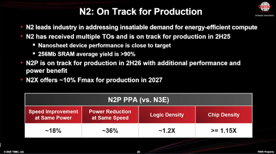
From the TSMC Symposium 2025:
1761407213413.png
https://www.tsmc.com/english/node/223# Technology Leadership Dr. Yuh-Jier Mii

N2X is for production in 2027, too late for Zen 6.
N2P is on track for production in 2nd half of 2026. This is start HVM, not first products with N2P delivered.

The numbers are N2P vs N3E. Why do you think TSMC is comparing not to N2?
 
Last edited:

basix

Senior member
Oct 4, 2024
276
547
96
I assume N2X gets compared to N2 vanilla on that slide. And as N2P already brings a Fmax boost, N2X won't bring too huge gains.

But anyways, the point is that the jump from N4P to N2P is much bigger than N2P to N2X. Maybe 80% of the overall Fmax gains TSMC states. So N2X might be good for Zen 6 desktop but it will not win the game.
 

reaperrr3

Member
May 31, 2024
136
394
96
yeah cuz it taped out a while ago on N2p.
Can we even consider N2P/X separate processes at all?
As far as I understood, one of the newer N3 chips (forgot if it was Snapdragon X2 or some Nvidia chip) uses N3P with some N3X transistors for clock-critical parts, so I'd assume this kind of mix is possible with N2P/X too and AMD would only design one 12C CCD, and not one N2P variant and one N2X variant.
 
  • Like
Reactions: Joe NYC