Zen 2 APUs/"Renoir" discussion thread

Page 22 - Seeking answers? Join the AnandTech community: where nearly half-a-million members share solutions and discuss the latest tech.

LightningZ71

Golden Member
Mar 10, 2017
1,627
1,898
136
That’s, what, largish hand held game system territory? Possibly something akin to a Switch 2 or small set top box?
 

NostaSeronx

Diamond Member
Sep 18, 2011
3,686
1,221
136
Isnt FFx = FireFlightx

I suspect it is actually
FF3 \ BGA \ 75 watt
8x Zen2 / 24 CU RDNA2 / GDDR6

FF1 => 100W | 4c Zen | 24 CU Vega | GDDR5

The main difference between Mero/Van Gogh is SE0/SE2 have two CUs disabled for one of them.

890F0X = VN (Early model = 20 CU w/ 24 CU on die?)
890F8X = MR (Late model = 24 CU active?)

The only ultra low power socket supporting DDR4/LP -> DDR5/LP is FT5 and its revisions within those TDPs:
pastedImage_1.png
And, those parts only have artists who relate to Dali and Pollock in America.

FT4 was the only socket for Nolan/Amur. The only parts to actually use any FF BGA in production is Fenghuang(East name)/Fireflight(West name) SoC.
 
Last edited:

Shivansps

Diamond Member
Sep 11, 2013
3,855
1,518
136
It may be the "first of the next gen of "flight sims, but it certainly doesn't represent the whole pantheon of games or even game engines. MSFS, like most new AAA games, has performance issues. Those issues seem to be independent of the hardware available. When 3900X's with 2080s have massive frame rate dips, there's more going on than "the hardware isn't good enough". That's an issue with game engine performance scaling. That the difference in overall performance of the 4700 and a system with the "minimum" spec of an RX570 is so minimal, it tells you right there that something, somewhere isn't scaling properly.

I will conceed one very important thing with MSFS, it is VERY texture heavy. It absolutely churns through VRAM and moves a lot of data back and forth from system RAM to VRAM. Since APUs still don't use a full unified memory model, there is going to be a lot of duplication of data in RAM, and a lot of needless copying back and forth, further clogging up the memory bus. I can suggest that, if you are going to attempt to play a game like MSFS with an APU, memory tuning and size are going to be crucial in getting anywhere near playable performance.
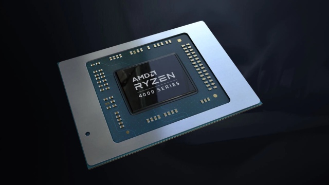
Again, i was not making an statement that every next gen game is going to be like this, it is a red flag, for all current hardware, thats all. And i know it has issues.

About your memory theory, what i saw, so far, from several sources, puts the RX550 GDDR5 below 3400G/4750G IGPs, i think this thing may be using a lot of gpu compute.
 

NostaSeronx

Diamond Member
Sep 18, 2011
3,686
1,221
136
Wait, it says Navi there.
Navi 2x = RDNA 2, it isn't wrong other than missing; Navi 1x = RDNA, Navi 2x = RDNA2, Navi 3x = RDNA3.

We know from leaks that the GPU in Van Gogh/Mero is related to Navi21 "Sienna Cichlid" which is a RDNA2 GPU of Navi.

If we are looking for a ULP RDNA2 chip it needs to be based off Navi22. Which means Van Gogh/Mero replaces Cato & Fireflight, not RN/LN/CN & Dali/Pollock.
renoir.png

Renoir solutions already supports 4.5W operation and the ability is carried over into 17h 68h-6Fh and 19h 50h-5Fh. With 19h 40h-4Fh replacing 17h 90h-9Fh.

Xbox X-series SoC (Arden) => VN/MR APUs
17h 80h-8Fh(14 instances x4), 17h 90h-9Fh(8 instances x3)

Technically we already have been forced fed what VN/MR is => Microsoft's new cheaper next-gen Xbox Series S console has a 3.8GHz 8-core Zen 2 CPU, but GPU only has 20CUs clocked at 1.55GHz.
 
Last edited:

LightningZ71

Golden Member
Mar 10, 2017
1,627
1,898
136
Nosta believes that Vega 7 is derived from Vega as it exists in the Mi100 compute card. I believe that it is a clock increased refinement of Vega 8 in Renoir, but with one CU removed to save die space because they are still on N7 (improved), but switched to the larger Zen3 cores with unified L3 and are trying to keep the die smallish.
 

NostaSeronx

Diamond Member
Sep 18, 2011
3,686
1,221
136
Nosta believes that Vega 7 is derived from Vega as it exists in the Mi100 compute card.
No I believe the slide is a fat fake.

Renoir (8C-1.8)/(8CU-1.75)
Lucienne w/ CZN BIOS blobs (8C-1.9)/(8CU-1.85)
Cezanne w/ N5

Cato is derived from Xbox One S => RE8125FEG84HU/RE8120FEG84HU @ ~240 mm2
Fireflight => Only in Subor Z+ @ ~397 mm2 (FF socket = Fireflight socket)

Van Gogh is the successor to both and is Lockhart in Xbox Series S. It isn't a low power part => Cato 135W and Fenghuang 100W.
With it being the traditional Picasso to Bristol die size @ 210 to 250 mm2.

The RDNA2 IP in Van Gogh is the same in Navi21, thus it has the 4xINT4/8xINT4 instructions. Which means it supports a faster GPU-accel for MIVisionX/MIVisionX Lite.

Lucienne/Mero are identical. Mero is a buffer for a large 5nm APU. Lucienne is a buffer for a medium 5nm APU. However, there is only one small 6nm APU with it's next entry being a 4nm APU @ TSMC. Hence, the small APUs stay cost-effective on leading edge; N5 is 1/3rd more expensive than N7, N6 is less expensive than N7.

This as well:
SP3 => SP5
AM4 => AM6
 
Last edited:

NostaSeronx

Diamond Member
Sep 18, 2011
3,686
1,221
136
Luciene is a semi-costum for cromebooks -link is in original post-
A couple said that for Dali/Pollock as well. But, they released in the normal stream.

AMD 3015e => Pollock

Lucienne is a refresh of Renoir.

Like this:
July 7, 2019 - 3900X => July 7, 2020 - 3900XT

Thus:
1/6/2020 - Ryzen 7 4800U => 1/6/2021 Ryzen 7 4820U/4850U/4870U, etc. It should also bring in the e-suffix for sub-10W FP6.

Going up 300 MHz on the CPU-side is over my estimation since it should come with that 1.85 GHz gpu clock as well. LCN should get mistaken as CZN do to it sharing CZNpi.
 
Last edited:
  • Like
Reactions: Olikan

CluelessOne

Member
Jun 19, 2015
76
49
91
My work laptop has Ryzen 7 PRO 4750U (and DDR4 3200 MHz 32GB in dual channel mode) and it is absolutely fantastic. The leap from dual core i5 Haswell is incredible. It also annihilates my 3770K.
Which model was it? The laptop I mean.
 

moinmoin

Diamond Member
Jun 1, 2017
4,952
7,663
136
Hm, didn't follow the development on Thunderbolt in AMD laptops, is Lenovo Yoga Slim 7-14ARE the first AMD laptop to include Thunderbolt 3?


mmaenpaa

Member
Aug 4, 2009
78
138
106
Hm, didn't follow the development on Thunderbolt in AMD laptops, is Lenovo Yoga Slim 7-14ARE the first AMD laptop to include Thunderbolt 3?

They corrected article, no TB3 so far on AMD laptops. I've installed a few Lenovo E15 (R7 4700U) & X13 (R5-4650U) laptops and I must say these things feel ridiculously fast :)
 

moinmoin

Diamond Member
Jun 1, 2017
4,952
7,663
136
They corrected article, no TB3 so far on AMD laptops.
Pfff, that's quite the dent into notebookcheck's credibility. I was always assuming they post and watermark their own photos, not use those of manufacturers. That they showed and are still showing pictures of the Intel model in an article about the AMD model should be a complete no go, after all after this mix up who knows what else differs between the models.
 

A///

Diamond Member
Feb 24, 2017
4,352
3,154
136
I know of two AMD mobos at the moment that support TB3 out of the box. I feel like TB3 is going to go the way of eSATA and USB4 will encapsulate it as a more easier qualification standard. Unless USB4 is for data i/o only.
 

NostaSeronx

Diamond Member
Sep 18, 2011
3,686
1,221
136
Just some speculation via the expectation Zen2 APU thread.

x200yz => 2 cores, 8 compute units
x400yz => 4 cores, 12 compute units
x600yz => 6 cores, 16 compute units
x800yz => 8 cores, 20 compute units
xA00yz => 8 cores, 24 compute units

z = 65W Sustained TDP/105W PPT Max or 95W Sustained TDP/135W PPT Max
y = APU letter
x = Gen number

1. DDR5(Socket)/GDDR6(BGA) only; HEDT APU family isn't going into laptops.
2. PCIe Gen4 GFX/GPP lanes.
3. 2e monkier for both CPU/GPU.
 
Last edited:

JustMe21

Senior member
Sep 8, 2011
324
49
91
It's been almost a month and a half since AMD release the OEM/PRO 4000 APUs, so when are they going to release the retail 4000 APUs?