The number I've seen floating around in the past 2 years was between $10,500 and $11,000 for N7, and around $18,000 for N5 for what it's worth. These were from decently old leaks from a large volume customer (that we never found out the name of). Every time this comes up, the numbers drift back in that direction. I believe the last number I saw was $10,818 for N7. I don't remember the exact N5 number. Add in a 10% increase due to the supply chain and inflation nonsense and you land at about $11,900 or so for N7. The defect rate of N7 was listed as being under 8%, which means > 92% of dies were defect free. N6 and N5 apparently have an even better defect rate.
I do not know the accuracy of these numbers, of course, but my gut tells me they are close to correct for a large-ish customer.
Those numbers are too high.
For the past 18 months, the most widely cited numbers for TSMC's wafer prices have been sourced from a research paper published in April 2020 by Georgetown University's Center for Security and Emerging Technology (CSET) and authored by Saif M. Khan and Alexander Mann. The full document is available here:
https://cset.georgetown.edu/publication/ai-chips-what-they-are-and-why-they-matter/
The following chart is located in "Appendix D: Chip Economics Model":
Being an academic research paper, the authors were very forthright with disclosure regarding the methodology of their cost model. Saif Khan, the primary author,
has also joined forum discussions to further clarify the source of the numbers, weigh in on the pros and cons of their particular model, and attempt to establish the overall accuracy and/or suitability for use.
Scotten Jones of IC Knowledge, who has been working on what is arguably the best strategic cost and price model in the industry for 20 years, published a detailed follow-up at SemiWiki:
https://semiwiki.com/semiconductor-manufacturers/tsmc/292760-leading-edge-foundry-wafer-prices/
The conclusion is:
This brings us to the key question, how accurate are the row 7 “Foundry sale price per wafer” values in the paper and the answer is not very. There is basically an error slope to the results with the 90nm prices being too low and at 5nm the prices are too high.
Your theory that prices would increase as a node matures is completely incorrect. The most significant contributor to wafer cost for a new node is capital depreciation. Because this is calculated as depreciation divided by wafer-outs per node per quarter, as the process ramps, utilization increases, and cycle times drop, you have a generally declining capital cost spread across a significantly higher number of wafers after the node reaches HVM. While TSMC will pocket some of that cost reduction to maintain their company wide 51% gross margin, as capacity expands, prices generally need to go down in order to keep utilization as high as possible. Even with continuing strong demand and pretty much every fab at full capacity, semiconductors are still extremely price sensitive components.
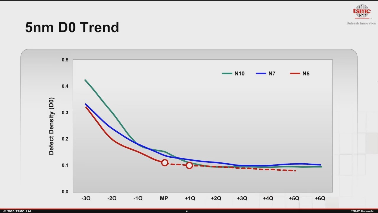
Defect density follows a curve that depends heavily on the maturity of the particular manufacturing process and cumulative number of wafer starts. It also shouldn't be a factor when it comes to foundry wafer pricing. Risk starts are called that for a reason, and generally that risk falls on the customer. TSMC tends to be somewhat forthcoming with their D0 numbers:
Yield percentage calculations depend heavily on the die size and method used to obtain them as well as the D0 at that particular time; you can't just quote a number for a wafer. Also, designs that take the expected defect density into account and make affordances for manufacturability can yield a significantly higher number of sellable dies.