Discussion Intel current and future Lakes & Rapids thread

Page 576 - Seeking answers? Join the AnandTech community: where nearly half-a-million members share solutions and discuss the latest tech.

repoman27

Senior member
Dec 17, 2018
342
488
136
Their 7nm cost per wafer is significantly overvalued.

5nm isn't bad though. More likely than not it's just by chance though. Fact of the matter is that cost per transistor has been rising since 16/14nm nodes.
I don't understand the context of that first sentence. And once again, you provide zero evidence to support your assertions here.
Also, you're being extremely generous by claiming it needs to be 70% higher cost per wafer to be a worse deal, as you're disregarding the poor SRAM scaling (1.2x) and analog scaling (1.1x) of N3. Look at A14 vs A13, only a 35% improvement to overall transistor density despite technically being a better shrink (1.8x logic, 1.35x SRAM can't remember analog logic), with N3 you'd see even less than that, more likely only a 20-25% improvement to transistor density at best.
You're absolutely correct on this point—I was only paying attention to logic densities. The yielded wafer cost would have to rise less than 25-35% to keep transistor prices the same overall. However, that's also why it makes sense for Intel to disaggregate the way they did with Meteor Lake and keep everything analog and as much cache as possible on Intel 7 or TSMC N5/N4.
 

Doug S

Platinum Member
Feb 8, 2020
2,263
3,514
136
Everyone has trouble getting EUV equipment. Unlike Intel who doesn't know how to use it, TSMC and Samsung are not getting enough EUVs. According to ASML, each 45k wpm requires 10~20 EUV scanner for 7~5nm nodes(3nm will need more), but ASML makes ~30 EUV scanners every year(Plans to boost to 60 by 2023 but not here yet).
So each year, ASLM can supply 100k wpm EUV fabs worldwide. The world lacks 15 EUV scanners in 2022 according to the source. Since Samsung bought more EUV than TSMC in 1st half of 2021, we can't say that TSMC got sufficient EUV by buying every EUV possible.

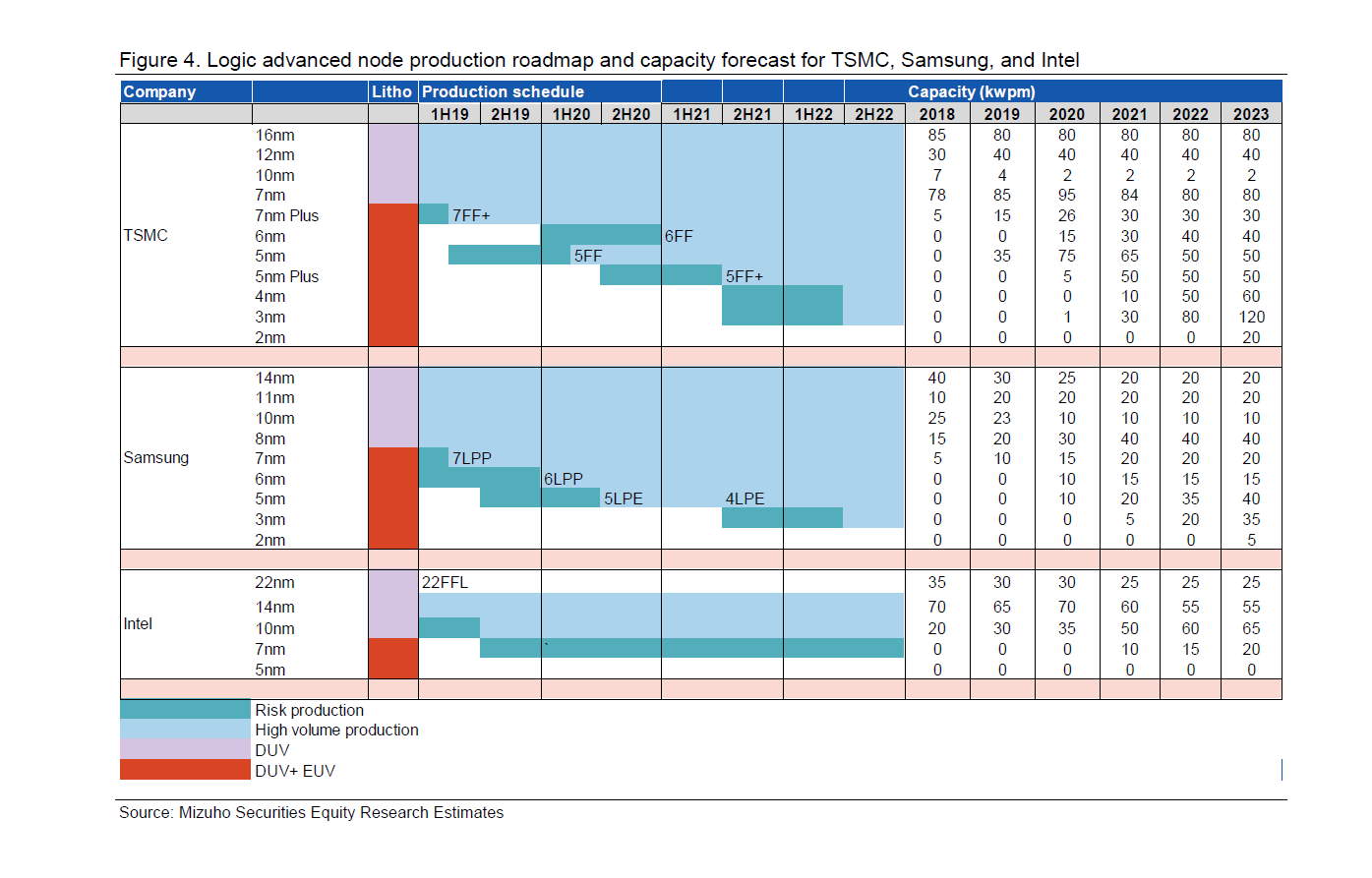
And now, DRAM makers are starting to purchase EUVs(2~10(?!) EUVs per 100kwpm) . In DUV days, TSMC alone had 100k~120k wpm for each leading-edge nodes. But now, that 100k will be separated to TSMC, Samsung and later, Intel.


These are ordered years in advance, so a difference like Samsung getting more than TSMC in the first half of this year doesn't say anything about whether TSMC got a "sufficient" number of EUV machines for their needs. It isn't like Samsung got up early on January 1st and placed put in a bunch of orders and too bad for TSMC who overslept. Foundries are probably taking delivery on orders they placed in 2018 or even earlier.

Since the orders are placed well in advance, but they don't have confirmed delivery dates until a lot sooner, foundries probably can't accurately plan number of wafer starts or possibly even node availability until they get those confirmed delivery dates from ASML. ASML doesn't so much have production targets, as production goals. If they can find a way to produce two or three more scanners than they had planned for that year, they will do so and foundries will be happy to take delivery a bit earlier than they had been told a year before when delivery dates were confirmed.

Supposedly when Intel had all their problems (before they replaced their CEO) they canceled orders from ASML. That's what led to speculation from some that Intel would no longer pursue advanced nodes and would go fabless in the long run. Given this was right around the time they made the deal for leading edge TSMC capacity my bet has always been that they traded those orders (i.e. "spots in line for delivery") to TSMC in exchange for being able to buy the capacity those scanners made possible for TSMC to add. TSMC has said they will be doing 30k N3 wpm in risk production and 105k wpm in full N3 production - about double N5's full production number. So Intel may get a lot of N3 slots, depending on how much of that wpm difference is accounted for by machines that Intel had ordered that TSMC is apparently getting instead.
 

Doug S

Platinum Member
Feb 8, 2020
2,263
3,514
136
Tell that to Apple who have already shipped:

200 million A14 @ 87.76 mm²
80 million A15 @ 107.7 mm²
20 million M1 @ 119 mm²
2 million M1 Pro @ ~250 mm²
1 million M1 Max @ ~424 mm²

All made on TSMC N5.

You're overestimating how many of the newest iPhones Apple sells versus "last year's model" and "two years ago" model and SE. You can google around and find a product sales mix for them, but from what I recall in the quarter after a new iPhone is released about 75% are the newest one, with that number decreasing over time until it is not all that much more than 50% in the quarter preceding a new iPhone release. There's no way they've shipped 200 million A14 and 80 million A15, I'd lop 25-35% off those A14/A15 numbers.

Still a lot, but your numbers would only be true if Apple stopped selling older models when a newer one came out. They get a lot of people saving $100 on that, and a fair number of the carrier deals for a "free phone" are getting last year's iPhone or an SE.
 
  • Like
Reactions: Tlh97 and Ajay

Doug S

Platinum Member
Feb 8, 2020
2,263
3,514
136
What makes you think either will be N3? They're skipping N3 in 2022 because of poor power/perf and density shrink relative to cost increase, especially compared to N4P. N3E is only going to be ready at the end of 2023/beginning of 2024, and so misses the production cycle for 2023 iPhone.

They aren't "skipping N3 in 2022 because of poor power/perf". They are "skipping" it for the same reason they skipped it this year - because it isn't an option available to them. N4P is the best available node at the time they need to begin taking delivery of tens of millions of A16s per month.
 
  • Like
Reactions: Tlh97 and Ajay

repoman27

Senior member
Dec 17, 2018
342
488
136
You're overestimating how many of the newest iPhones Apple sells versus "last year's model" and "two years ago" model and SE. You can google around and find a product sales mix for them, but from what I recall in the quarter after a new iPhone is released about 75% are the newest one, with that number decreasing over time until it is not all that much more than 50% in the quarter preceding a new iPhone release. There's no way they've shipped 200 million A14 and 80 million A15, I'd lop 25-35% off those A14/A15 numbers.

Still a lot, but your numbers would only be true if Apple stopped selling older models when a newer one came out. They get a lot of people saving $100 on that, and a fair number of the carrier deals for a "free phone" are getting last year's iPhone or an SE.
I was trying to be cognizant of sales mix. But I'm also basing that on 5 quarters of A14 shipments including iPads. Regardless, you can lop all you like off of my numbers and it still paints a pretty healthy picture of TSMC's N5 process.
 

Ajay

Lifer
Jan 8, 2001
15,454
7,862
136
Still a lot, but your numbers would only be true if Apple stopped selling older models when a newer one came out. They get a lot of people saving $100 on that, and a fair number of the carrier deals for a "free phone" are getting last year's iPhone or an SE.
Exactly. I switched carriers last year. I could get an SE for free, an 11XR for $200 and an iPhone 12 for $400. I went for the later because it supported 5G. So, selling multiple older generations (n-2 in the US I think), really helps keep Apple rolling along with extra sales from the App store and various annual packages of Apple music, TV+, storage, etc.
 
  • Like
Reactions: Tlh97

repoman27

Senior member
Dec 17, 2018
342
488
136
If we are to believe the Mizuho report, TSMC should have 120 kwpm of N3 alone by some point in 2023 (probably the end of the year, at this rate). That's 6x the projected wafer output of Intel 7nm/Intel 4 in the same timeframe. And (allegedly) Intel is only getting 20 kwpm of that N3 volume.

TSMC will also (allegedly) have 60 kwpm of N4 by that time. How much of that will be N4P is unknown since it isn't included in the only source I have, which is the good old Mizuho report.

Arrow Lake may be a refresh of Raptor Lake on 10ESF/Intel 7. If you think about it, they will not have a lot of N3 + Intel 4 to go around! And they have to share all that between Meteor Lake, Granite Rapids, and Arc/Xe. They are also getting some N6 and N5 (apparently) so some of their products may wind up on that.

If TSMC has this kind of available volume, do you think that is due to them being short on EUV equipment?

E09U5KvVoAAoYZC


The dates on N3 may be pushed back a little (Q2 2022 for N3 may become Q1 2023; not really sure) but still. 120 kwpm N3? 60 kwpm N4? They're going to equal Samsung and Intel's total output for Intel 7 + Intel 4 + 4LPE + 3GAE/3GAP.
The purpose of the Mizuho note is to encourage readers to buy ASML stock. ASML sells DUV as well as EUV equipment, and the investment note addresses both. The charts that everyone is fascinated by are included for context, to support the claim that ASML's products will see continued strong demand for the foreseeable future. Because ASML is the only game in town for EUV, and publicly report every unit delivered each quarter, that data is provided along with projections and an attempt to break down purchases by customer. They also include a production forecast for advanced nodes across ASML's top customers, which is the chart you referenced. Although that chart includes columns labeled "Capacity (kwpm)", those figures are clearly not the nameplate capacities for the fabs based on square footage, installed equipment, and support facilities. However, in most cases, they are completely reasonable estimates for fab utilization on each of the respective manufacturing processes. The utilization, not the peak capacity, is ultimately what drives demand for the products ASML sells.

Given that context, we see that Intel only has a single EUV node on the horizon: 7nm (a.k.a Intel 4). That process is facing a very long, slow ramp, and is only expected to achieve 20 kwpm utilization by 2023. Given the number of EUV layers used for Intel 7nm and the number of machines they have already taken delivery of, we shouldn't expect Intel to increase their EUV orders until 2023 at the earliest. That takeaway is echoed in the EUV shipment forecast. On the other hand, Intel will remain heavily reliant on DUV equipment throughout 2023, which also has upside for ASML because they are currently supply constrained in regard to EUV tools.

TSMC already has four EUV nodes in HVM and at least two more on the horizon for which they have considerable volume planned. They are currently the number one EUV customer and will remain so for the foreseeable future. However, while purchases of new EUV equipment will continue to increase, we should expect them to decelerate after 2021. Because they have by far the most EUV machines on order, they also face the most risk if ASML is unable to deliver on schedule.

TSMC N4P was not included in the chart because it hadn't been publicly announced yet, and I believe it's scheduled to arrive after N3. The report is from April 16, 2021, and judging by the projections for N4 and N3, the folks at Mizuho may not have been hip to the fact that the A16 was going to be on N4 and would arrive a quarter sooner than their estimate. Regardless, Intel can effectively have as many TSMC wafer starts as they care to pay for as long as they are somewhat flexible with scheduling. For instance, N4 is going to be pretty well booked by Apple for most of H1'22. I have a bit of trouble believing those N3 projections, but if they're even remotely right, there's no problem there at all. Intel can also run as many Intel 4 wafers as they can stomach until defect densities reach a reasonable level, and then they can probably crank it up to at least 45 kwpm before they need to wait on more EUV equipment.
 

repoman27

Senior member
Dec 17, 2018
342
488
136
They aren't "skipping N3 in 2022 because of poor power/perf". They are "skipping" it for the same reason they skipped it this year - because it isn't an option available to them. N4P is the best available node at the time they need to begin taking delivery of tens of millions of A16s per month.
Slight niggle, A16 will be on N4. N4P won't be available until shortly after N3.

TSMC expects the first products based on N4P technology to tape out by the second half of 2022.
 

Ajay

Lifer
Jan 8, 2001
15,454
7,862
136
Doesn't work that way. You order in 2023, who knows when you will get it. Maybe never. You are forgetting about Samsung who is also in the mix too.
Not never! ASML is like any other manufacturer with long lead times. You book the product in advance, they probably give an estimated delivery time subject to various conditions. Then you go into a FIFO and when ASML has an expected ship date (probably all the parts are in) you get a call from the sales rep to setup delivery. I would guess that with ASML overbooked, you have to lay down some cash up front, then pay it off after delivery and test.
 

repoman27

Senior member
Dec 17, 2018
342
488
136
Doesn't work that way. You order in 2023, who knows when you will get it. Maybe never. You are forgetting about Samsung who is also in the mix too.
I suppose it would have been more accurate to say "take increased deliveries of EUV equipment" rather than "increase their EUV orders", but nobody investing in ASML cares how it actually works. All they care about is when ASML recognizes revenue. The entire point of my post was that Mizuho only acknowledged Intel insofar as they are top 3 customer of ASML. Intel knows how to order the equipment that they need and who they are competing against.

Not never! ASML is like any other manufacturer with long lead times. You book the product in advance, they probably give an estimated delivery time subject to various conditions. Then you go into a FIFO and when ASML has an expected ship date (probably all the parts are in) you get a call from the sales rep to setup delivery. I would guess that with ASML overbooked, you have to lay down some cash up front, then pay it off after delivery and test.
Nah, they send you a confirmation email right away, but wait until your order actually ships before charging your credit card. Then a delivery truck shows up at some random time when you're not around and leaves your $150M EUV system sitting on the front porch.
 
Last edited:

DrMrLordX

Lifer
Apr 27, 2000
21,632
10,845
136
Because they have by far the most EUV machines on order, they also face the most risk if ASML is unable to deliver on schedule.

Yes, but that is an "if", not a "when". I see no evidence that TSMC (or Samsung, for that matter) has any particular reason to worry about their orders being fulfilled. The only thing we can reasonably know (or at least estimate) is whether or not a particular company has placed orders in time to bring particular EUV nodes into production according to schedule. TSMC and Samsung have placed their orders.
 

andermans

Member
Sep 11, 2020
151
153
76
@repoman27

This is a slide from Marvell (See here). Never realised a chart like this was public until just now.

It's pretty self explanatory.

View attachment 53562


Full wafer prices here:
too (same data AFAICT)

Note that cost per gate is very malleable. Just in that graph the raw cost/gate is going down in 10nm->7nm, but they account for gate utilization and some yields. Not really sure but if the utilization about power/heat density that would be a reason for companies to design their chips differently (e.g. for more accelerators for efficiency).

If I plug in some common chips with the 7nm wafer cost + die sizes and a 0.1 defect/cm2 I get the following prices:

* Navi21: ~85$
* Cezanne: ~20$
* Zen3 CCD: ~9$

Note that this is only defect density though I wonder what the performance yields would be. If this is anywhere close to correct though, then for most of the CPUs I'd think this is not that big of a deal. Like what is a + 4$ increase on a 200$+ product? I'd think market placement and hence the resulting demand would be way more impactful. If 3nm gives some performance/efficiency advantage (not sure what, compared to 4p. Maybe reduced wire length or other attributes being an advantage? Like a physically smaller cache could have lower latency to due wire delays) I could totally see it being worth it. I'd imagine the low cost CPUs (Atom,Pentium, Athlon) are the ones really impacted by this, since some of those are actually going in the 10-30$ range.

Or maybe 4p is preferred but if there is not enough/early capacity companies will divert to 3nm?
 

uzzi38

Platinum Member
Oct 16, 2019
2,632
5,959
146
Full wafer prices here:
too (same data AFAICT)

Note that cost per gate is very malleable. Just in that graph the raw cost/gate is going down in 10nm->7nm, but they account for gate utilization and some yields. Not really sure but if the utilization about power/heat density that would be a reason for companies to design their chips differently (e.g. for more accelerators for efficiency).

If I plug in some common chips with the 7nm wafer cost + die sizes and a 0.1 defect/cm2 I get the following prices:

* Navi21: ~85$
* Cezanne: ~20$
* Zen3 CCD: ~9$

Note that this is only defect density though I wonder what the performance yields would be. If this is anywhere close to correct though, then for most of the CPUs I'd think this is not that big of a deal. Like what is a + 4$ increase on a 200$+ product? I'd think market placement and hence the resulting demand would be way more impactful. If 3nm gives some performance/efficiency advantage (not sure what, compared to 4p. Maybe reduced wire length or other attributes being an advantage? Like a physically smaller cache could have lower latency to due wire delays) I could totally see it being worth it. I'd imagine the low cost CPUs (Atom,Pentium, Athlon) are the ones really impacted by this, since some of those are actually going in the 10-30$ range.

Or maybe 4p is preferred but if there is not enough/early capacity companies will divert to 3nm?
As I'm pretty sure I remember Ian points out in that video, the wafer pricing figures given there were long before N7 actually ended up in mass production.

I wouldn't assume that wafer pricing is accurate for when the node actually debuted.
 

andermans

Member
Sep 11, 2020
151
153
76
As I'm pretty sure I remember Ian points out in that video, the wafer pricing figures given there were long before N7 actually ended up in mass production.

I wouldn't assume that wafer pricing is accurate for when the node actually debuted.


Somewhat agree, but the price per 100M gates is exactly the same as your graph (common source?), so to exactly the same extent that is unreliable. And given the general trend I doubt it would be off by >2x which would mean the order of magnitude is still informative.
 

uzzi38

Platinum Member
Oct 16, 2019
2,632
5,959
146
Somewhat agree, but the price per 100M gates is exactly the same as your graph (common source?), so to exactly the same extent that is unreliable. And given the general trend I doubt it would be off by >2x which would mean the order of magnitude is still informative.
That I agree with. It's certainly MUCH better than the previously quoted $14K per wafer if nothing else.
 

Doug S

Platinum Member
Feb 8, 2020
2,263
3,514
136
That I agree with. It's certainly MUCH better than the previously quoted $14K per wafer if nothing else.

When those prices were quoted matters a lot though. When N7 was new probably $14K was accurate. Today probably $7K or even less is accurate, because TSMC has heavily depreciated their N7 buildings and equipment. Apple and the other early adopters are paying down that fixed cost in exchange for getting N7 wafers sooner than those willing to wait a couple years.
 

repoman27

Senior member
Dec 17, 2018
342
488
136
The actual source of those tables is International Business Strategies, Inc. Could someone kindly explain what the "Gates/mm²" metric represents? How is "Gate utilization" calculated? How is "Parametric yield impact" derived and why it is being applied at this stage of the calculation? Try doing the math using the numbers in the table and see if you obtain consistent results.

IBS Cost Per Gate.png

Dr. Handel H. Jones who comes up with this stuff clearly landed some big-name clients, so these numbers may have some legitimate applications, but they aren't the same as straight up transistor cost.
 
  • Like
Reactions: lightmanek

andermans

Member
Sep 11, 2020
151
153
76
When those prices were quoted matters a lot though. When N7 was new probably $14K was accurate. Today probably $7K or even less is accurate, because TSMC has heavily depreciated their N7 buildings and equipment. Apple and the other early adopters are paying down that fixed cost in exchange for getting N7 wafers sooner than those willing to wait a couple years.

Note that these numbers were presented (among others) in a ~2016 talk so these should have been pre-order numbers before the process landed. I'd suspect that is closer to "new" than "fully depreciated".

@ repoman27: The gates used for the cost estimate is "Actual used gates/mm2" (or rather "gates/wafer" which is that multiplied by ~63630 , probably the wafer area) which is "gates/mm2 * Gate Utilization * Parametric yield impact".

Not sure what drives gate utilization (maybe heat density?) but parametric yield utilization is yield that doesn't consider defects (i.e. catastrophic failures) but considers process variations that cause some elements to perform worse than required.

One question with parametric yield is how often that results in unusable chips vs. just chips that you would sell with a lower bin (e.g. worse clock speed) or with the problematic parts of the chip disabled (just as you do with defects).
 

repoman27

Senior member
Dec 17, 2018
342
488
136
Note that these numbers were presented (among others) in a ~2016 talk so these should have been pre-order numbers before the process landed. I'd suspect that is closer to "new" than "fully depreciated".

@ repoman27: The gates used for the cost estimate is "Actual used gates/mm2" (or rather "gates/wafer" which is that multiplied by ~63630 , probably the wafer area) which is "gates/mm2 * Gate Utilization * Parametric yield impact".

Not sure what drives gate utilization (maybe heat density?) but parametric yield utilization is yield that doesn't consider defects (i.e. catastrophic failures) but considers process variations that cause some elements to perform worse than required.

One question with parametric yield is how often that results in unusable chips vs. just chips that you would sell with a lower bin (e.g. worse clock speed) or with the problematic parts of the chip disabled (just as you do with defects).
Yeah, sorry, I should have indicated that those were mostly rhetorical questions. My issue is that the numbers I questioned are all completely arbitrary, unless someone can point to where they came from. 39% of your "gates" are lost to defects on 16/14nm? Whose process? Which process? When? What yield model? At what die size?