The cost to Intel now is basically like 200-300 bucks tops. You won't see that on the accounting because they are including money Intel spent 5 years ago.
You realize that $200-300 is on the low side for just the cost of the raw wafer and consumables, right? Even if all of Intel's 10nm equipment and facilities were 100% depreciated at this point, which they are not, the loaded cost would still include labor, facility operating costs and maintenance. Yields on 10nm (Intel 7) appear to be OK at this point, but the process still involves copious multi-patterning which leads to long cycle times. Throughput and yields will never be able to match 14nm, so it will always be a more expensive node. I challenge you to find a credible analyst who would peg the Intel 7 yielded wafer cost in Q4'21 at less than $3000.
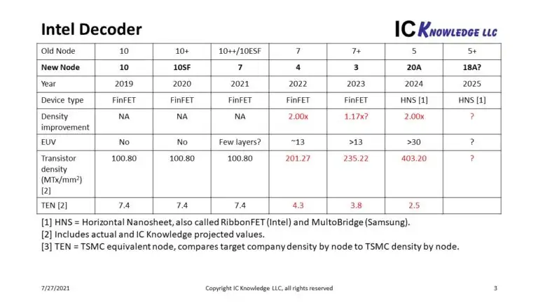
Intel 4 is absolutely comparable to edge TSMC nodes. Transistor density on Intel 4 is higher than TSMC N5.
Transistor density on Intel 7 can be comparable with TSMC N7.
Yes, Intel 4 will be more dense than TSMC N5. However, TSMC N3 will be 1.4x denser and enter HVM right around the same time as Intel 4. N5 products have been shipping in high volume for over a year, and 430 mm² monolithic SoCs are available today. In terms of process maturity, Intel 7 is up against TSMC N5/N5P which is 1.65x denser.
You guys talking about cost bugs me. Go look at TSMC’s financials, specifically, margins. Intel’s costs are far below what TSMC charges customers. Intel is vertically integrated.
Intel’s biggest worry for the forseeable future is their lack of EUV machines. They control the majority of everything else. They make more money per chip than AMD does. They don’t have the supply constraints AMD does (this isn’t to say they don’t have supply issues, but they don’t compete with others for a given node).
The only reason Intel is using TSMC is due to EUV. Intel did not order enough EUV machines, which limits the number of chips they can make on Intel 4 and below. They are working to rectify that going forward.
If TSMC N3 and Intel 4 were to have equivalent yielded wafer costs, a TSMC gross margin of 30% would still provide Intel with the same transistor cost. Overall, TSMC's gross margins are currently hovering above 51%, but the margins on the bleeding edge nodes are almost certainly lower. And because TSMC is way higher volume, generally has lower operating costs, and has had better yields recently than Intel, their yielded wafer costs will likely be lower than Intel's. So the price difference isn't going to be all that much in the end. Being an IDM doesn't mean you get your fabs for nothing and your wafers for free. It's also darn near impossible to make leadership products if you aren't using the best available process, which is why Intel killed it for over a decade when they had a monopoly on manufacturing that was way ahead of what everyone else had.
Intel 4 will be Intel's first manufacturing process to use EUV, and it won't enter HVM until H2'22. It will use EUV lithography for 12 layers. Intel will have 12-16 EUV machines installed up and running by then, enough to easily accommodate 45K WSPM. Thus far, they have only taped out a single 38 mm² client compute tile on that node, and announced that the Granite Rapids server parts, ostensibly due out by the end of 2023 will also use Intel 4 in some capacity. So while everyone on the internet keeps parroting that Intel is constrained by a lack of EUV equipment, I see $2B worth of EUV machines sitting around depreciating while utilization is nowhere near at full capacity.
The Mizuho Securities note that everyone uses as evidence of Intel's shortage of EUV equipment was a buy rating for ASML, and never once insinuated that Intel was underinvesting. That might have started with Daniel Nenni over at SemiWiki.