CakeMonster
Golden Member
I'd love to see a re-review of the findings with regards to the inter-core and inter-ccx latencies compared to Z4 when there are new AGESA/BIOS'es out and chipset drivers and Windows are properly updated.
Clock is ticking. AMD needs to get the fixed AGESA out the door BEFORE Arrow Lake launch.I'd love to see a re-review of the findings with regards to the inter-core and inter-ccx latencies compared to Z4 when there are new AGESA/BIOS'es out and chipset drivers and Windows are properly updated.
And what needs fixing? CCD to CCD latency? Was anyone able to correlate poor performance in this synthetic test with impact on any particular workload? Or is there something else that needs fixing? Chips&Cheese did one article long time ago https://chipsandcheese.com/2021/06/...to-core-latency-and-the-role-that-locks-play/ let me quote the conclusion:Clock is ticking. AMD needs to get the fixed AGESA out the door BEFORE Arrow Lake launch.
That is not to say such workloads do not exist, it might be also that C&C test approach was flawed or their game selection insufficient but anyway this synthetic test got lots of attention because of huge regression but I am unaware of anyone who was able to successfully link that to real world perf regression.Typically games have around 20-30 per 10000 instructions suffering a L3 cache miss, which means that games are much more bound by memory latency than lock latency. If you picked an instruction at random, it’s 20-30 times more likely to miss L3 than require a core to core transfer. The situation is more skewed for very parallel productivity workloads like Cinebench, where L3 misses happen about 80x as often as core to core transfers. So in conclusion, a core to core latency test using locks isn’t very indicative of how a CPU will perform with real world usage either of games or productivity workloads. Core to core latency is merely one part of a CPU’s overall performance, and plays a small role compared to other factors like the performance of a CPU’s cache and memory hierarchy.
In Zen you also suffer 1c latency penalty when you shift data from scalar / int register file to fp/simd register file if I understand documentation correctly. But this penalty is different to the penalty suffered exclusively by otherwise 1c latency SIMD ops.Alpha has that additional latency when instructions has to cross register file. Scheluder, in case of Alpha with help of programmer, tries to keep dependent instructions on same side of register file. But in situations like when there is 3 adds to scheluded in clock for 2+2 alu configuration one instruction needs to take wrong side and from that result dependent instructions see one cycle latency penalty. When scheluder can isolate dependent instructions to their own sides full thoughput can be maintained without any penalties.
Anything that AMD hasn't been able to do so far. I don't know what their TODO list for Zen 5 related AGESA improvements looks like but they better get to it fast. Also, if they release the X870E/X870 chipsets soon, those may also help performance a bit when used with Zen 5 optimized EXPO kits. And of course, if they are able to release the new X3D SKUs, that would further improve their standing in benchmarks.And what needs fixing?
Agree, 6400MT/S 1:1 must be the new "sweet spot", anything less is robbing the efficiency gains from Zen 5, also help in the market fight with Intel's upcoming arrow lake.Clock is ticking. AMD needs to get the fixed AGESA out the door BEFORE Arrow Lake launch.
Fabric clock sweet spot is 2000MHz, CCD to IOD link is 32B/c -> max bandwidth 64GB/s. If you are lucky you get 70,4GB/s with 2200MHz.Agree, 6400MT/S 1:1 must be the new "sweet spot", anything less is robbing the efficiency gains from Zen 5, also help in the market fight with Intel's upcoming arrow lake.
AVX-512 workloads using 512-bit registers will see benefit. They are the ones most in need of any extra bandwidth compared to the same instructions executing on Zen 4.In other words, the new sweet spot will be meaningless to 1 CCD SKUs.
Ok, maybe I wasn't clear enough. The CCD to IOD interface limits you to 64GB/s, while 6000MT/s DDR5 setups provides theoretical 96GB/s. Since CCD to IOD bandwidth is the limiting factor here, it doesn't matter how fast your DRAM is if you saturate CCD to IOD link first [probably better to have a bit higher for various contoller related overheads].AVX-512 workloads using 512-bit registers will see benefit. They are the ones most in need of any extra bandwidth compared to the same instructions executing on Zen 4.
AVX512 would love to use the bandwidth but it won't be able to.

 www.igorslab.de
Let me quote myself:The big Ryzen 7000 Memory and OC Tuning Guide - Infinity Fabric, EXPO, Dual-Rank, Samsung and Hynix DDR5 in Practice test with Benchmarks and Recommendations | Page 7 | igor´sLAB
AMD’s new Ryzen 7000 desktop CPUs, based on the Zen4 micro-architecture, still use the same chiplet design as their predecessors, with a few small but not negligible changes. Igor already gave details…
If one is able to get DDR5-6400 CL30 or lower working at 2133 IF with a high end DDR5-8200 RAM kit, AVX-512 WILL see gains. May not be as much as one would like but going for 6400 MT/s won't be a total waste over stock DDR5-6000 CL30. In AIDA64, that's 13% copy, 12.6% read and 14.2% write memory bandwidth gains. Not insignificant by any means.
Thanks for finding measurements that confirm this hypothesis😉 It's 7950X so 2 CCD SKU using AIDA that uses both CCDs😉In other words, the new sweet spot will be meaningless to 1 CCD SKUs. Only 2 CCD SKUs will be able to benefit provided you can engage both CCD dies. When it comes to bandwidth, at least.
Thanks for finding measurements that confirm this hypothesis😉 It's 7950X so 2 CCD SKU using AIDA that uses both CCDs😉

Let me quote myself once again:SkatterBencher #78: Ryzen 7 9700X Overclocked to 5860 MHz - SkatterBencher
We overclock the AMD Ryzen 7 9700X to 5860 MHz with the ASUS ROG Crosshair X670E Hero motherboard and AIO water cooling.skatterbencher.com
DDR5-6400 with tuned memory timings and IF @ 2200 on a 9700X yielding above 20% improvement in V-Ray and AI Bench, both of which presumably use AVX-512.
I have never said timings are not important. In fact they are more important than the pure bandwidth for single CCD SKUs due to IF limitation. Second if you read through his article paying some attention you will see that:In other words, the new sweet spot will be meaningless to 1 CCD SKUs. Only 2 CCD SKUs will be able to benefit provided you can engage both CCD dies. When it comes to bandwidth, at least.
So this 20 % AI Benchmark is not thanks to memory alone. The results shown are 9700X PBO + MEMORY EXPO vs 9700 Stock at 4800MHz RAM.Despite the Ryzen 7 9700X having only 8 cores, the performance is restricted by its maximum power to 65W. By enabling PBO, we can easily double the power budget in all-core workloads. Combined that with enabling higher memory speeds and it translates into significant performance gains across the board. The Geomean performance improvement is +4.04%, and we get a maximum improvement of +18.07% in the AI Benchmark.
Let me quote myself once again:
I have never said timings are not important. In fact they are more important than the pure bandwidth for single CCD SKUs due to IF limitation. Second if you read through his article paying some attention you will see that:
So this 20 % AI Benchmark is not thanks to memory alone. The results shown are 9700X PBO + MEMORY EXPO vs 9700 Stock at 4800MHz RAM.
I get you really want to prove your point Igor, but now it turns into pure spam of hastily thrown links that are supposed to validate what you say. I will drop the subject now in order not to deteoriate the thread further.
If 6000 MT/s is the so called "sweet spot" then why do Tech tubers like Tech YES City conduct testing between 9700X, 7700X & 7800X3D with 6200 MT/s? are they cheating or something?Fabric clock sweet spot is 2000MHz, CCD to IOD link is 32B/c -> max bandwidth 64GB/s. If you are lucky you get 70,4GB/s with 2200MHz.
For DDR: 6400MT/s with 128b(16B) bus is 102GB/s. With current sweetspot of 6000MT/s you are at 96GB/s.
In other words, the new sweet spot will be meaningless to 1 CCD SKUs. Only 2 CCD SKUs will be able to benefit provided you can engage both CCD dies. When it comes to bandwidth, at least.

 chipsandcheese.com
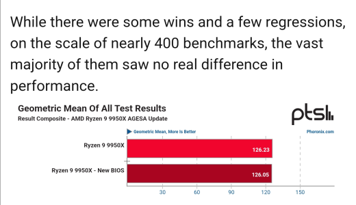
I did not see a median or average speedup, but it looks like ~10% faster.Phoronix benchmarked the new AMD BIOS: https://www.phoronix.com/review/amd-9950x-agesa-1202
Geomean is at the end, no difference.I did not see a median or average speedup, but it looks like ~10% faster.
the word Geomean does not exist on page 3. The power is identical though, that's at the end.Geomean is at the end, no difference.

the word Geomean does not exist on page 3. The power is identical though, that's at the end.
How I missed that is a mystery, sorry,Here
16.5 |
12.1 |
-10.3 |
9.9 |
9.8 |
8.7 |
7.9 |
-7.9 |
7.5 |
6.9 |
6.2 |
5.5 |
5.3 |
-4.9 |
4.8 |
-4.4 |
4.4 |
4.2 |
4.1 |
3.9 |
-3.8 |
3.8 |
-3.7 |
3.6 |
3.6 |
-3.5 |
-3.4 |
-3.4 |
-3.4 |
3.3 |
3.3 |
3.1 |
3 |
3 |
2.9 |
-2.9 |
-2.8 |
2.7 |
2.7 |
2.7 |
-2.6 |
-2.5 |
2.4 |
-2.3 |
-2.3 |
-2.3 |
2.3 |
2.2 |
-2.2 |
2.2 |
-2.2 |
-2.1 |
-2.1 |
2.1 |
2 |
2 |
2 |
1.712281 |