The Intel Atom Thread

Page 211 - Seeking answers? Join the AnandTech community: where nearly half-a-million members share solutions and discuss the latest tech.

coercitiv

Diamond Member
Jan 24, 2014
6,185
11,852
136
Is this kind of reply really necessary? His question was a fair question. Chill.
Someone popping up in a thread and deciding to casually ask people why they even bother discussing the subject? Look what happened next, we're already offtopic and enjoying a presentation on the merits of emulation in a thread about x86 Atom cores.

But let me ask you: do you think there's any reason to consider Atom?
 

DrMrLordX

Lifer
Apr 27, 2000
21,617
10,826
136
Atom was briefly interesting when Goldmont was new. Then Intel's process tech stagnated and the little Atom crew got put on the backburner when it came to 10nm wafer supplies (apparently). So the logical growth of Atom away from a bad mobile chip (Baytrail) and towards a low-power multifunction chip with good bang/buck was stunted. Sad, really, 'cuz Gracemont could be pretty interesting on its own, in the right applications.
 

TheGiant

Senior member
Jun 12, 2017
748
353
106
IMO gracemont will be "fast enough" at let's say 3,5GHz to handle all the ligher worloads in apps and windows/corporate bloatware, antivirus etc....
any info on Gracemont die size? predicted power/freq curve?
 

DrMrLordX

Lifer
Apr 27, 2000
21,617
10,826
136
IMO gracemont will be "fast enough" at let's say 3,5GHz to handle all the ligher worloads in apps and windows/corporate bloatware, antivirus etc....

Remember that Gracemont allegedly has IPC parity with Skylake. No idea on the amount of space Gracemont requires on the core, but if you look at how large Tremont is on Lakefield, Tremont is tiny.
 
  • Like
Reactions: geegee83

coercitiv

Diamond Member
Jan 24, 2014
6,185
11,852
136
For a sense of relative size, the ratio between big and little cores in Lakefield is roughly around 1:4.

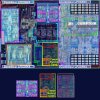
A picture helps more with the scale of things:

lakefield.jpg
 
  • Like
Reactions: geegee83

DrMrLordX

Lifer
Apr 27, 2000
21,617
10,826
136
@coercitiv

Right, the question is: how much larger is Gracemont? It's sad that Intel could probably get high yields out of 8c (or higher!) Tremont parts but still can't bring them to market for . . . reasons. Stranding a lot of their network/comm appliances and other products in the process.
 

ehume

Golden Member
Nov 6, 2009
1,511
73
91
The reason for following an Atom thread is that back in 1/12, MS was selling an HP laptop for $180 - a bargain at the time. And that is w/ Widows installed. True, an 11-inch screen limited its usefulness, but it was fine for viewing conference presentations/slides and for making notes.
 
  • Like
Reactions: spursindonesia

IntelUser2000

Elite Member
Oct 14, 2003
8,686
3,785
136
Right, the question is: how much larger is Gracemont? It's sad that Intel could probably get high yields out of 8c (or higher!) Tremont parts but still can't bring them to market for . . . reasons. Stranding a lot of their network/comm appliances and other products in the process.

Uhh, what do you think Snow Ridge is using?


:)

By the way Bay Trail was quite competitive. It lost to Apple SoCs at the time but outperformed standard ARM ones.

For a sense of relative size, the ratio between big and little cores in Lakefield is roughly around 1:4.

A picture helps more with the scale of things:

The FP/SSE units in Sunny Cove are almost as large as the entire Tremont core that includes the dual 128-bit SSE, but I believe the one in Gracemont will be far smaller due to different focus even if it moves to AVX2 and 256-bit.
 
Last edited:

IntelUser2000

Elite Member
Oct 14, 2003
8,686
3,785
136
Pretty sure Snow Ridge was still delayed. Along with Elkhart Lake. Did Intel ever get it out to market in quantity?

Where are you getting this from? It was launched back in February and they said they expect to have 40% MSS by 2021. How will they do that if they haven't even shipped yet?

Yes, they are very much shipping.

This is from Q2 report: ...and Intel’s portfolio for 5G network infrastructure gained customer momentum, most notably the 10nm-based Intel Atom P5900 for wireless base stations.
 
Last edited:

Dayman1225

Golden Member
Aug 14, 2017
1,152
974
146
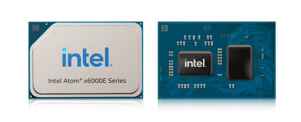
As of today Intel has offcially launched "Elkhart Lake". 10nm Atoms focused on the embedded/IoT market.

Intel Launches 10nm Atom Embedded CPUs: Elkhart Lake Now Available - AnandTech

Intel Announces Atom x6000E Series "Elkhart Lake", 11th Gen Core Tigerlake-UP3 - Phrononix

Intel Announces 10nm SuperFin Atom x6000E Elkhart Lake, Celeron and Pentium CPUs - Tomshardware

Elkhart Lake ranges from 2 - 4 cores and 4.5w to 12w and interestingly it is based on the 10nm SF process unlike SnowRidge and Lakefield so that means Tremont is designed for 10+ and 10SF and perhaps even 10ESF for future products.
image.php

Intel's claimed performance improvements:

  • 1.7x ST Improvement (Pentium J6425 vs Pentium J4205 in Spec2006)
  • 1.5x MT improvement (Pentium J6425 vs Pentium J4205 in Spec2006)
  • 2x GFX improvement (Pentium J6425 vs Pentium J4205 in 3DMark 11)
jM6BMeGPDwrQYYxuScYtm8-970-80.png.webp

Based on the pictures provided Ian Cutress from Anandtech tried to estimate die sizes (as they are PR photos take with grain of salt) his calculations were:
  • CPU die (left): 9.169 mm * 6.394 mm = 58.63 mm2
  • PCH die (right): 6.369 mm * 9.778 mm = 62.27 mm2
Another Interesting note that the Intel PSE (Programmable Services Engine) ships with an Arm Cortex M7 core:

Intel states that it has >=100 partners committed to releasing products with these processors.
 
Last edited:
  • Like
Reactions: Tlh97 and Kaido

moinmoin

Diamond Member
Jun 1, 2017
4,944
7,656
136
Since the Atoms are SoC a chipset shouldn't be needed, so what exactly is that huge PCH needed for? Is that where the ARM Cortex M7 resides? Or is "SoC" a misnomer for this particular Atom? (Note that AT's text description of the PCH capabilities doesn't seem to match the diagram of the reference platform above it.)
 

IntelUser2000

Elite Member
Oct 14, 2003
8,686
3,785
136
ARK page doesn't say SuperFin.

Also 70% over Apollo Lake in ST and 50% in MT is not a lot. That suggests similar performance to Gemini Lake in ST and MT.

And what's up with the separate PCH? So Jasper Lake will be a different config? They needed the additional features is that it?
 

mikk

Diamond Member
May 15, 2012
4,133
2,136
136
This is what Anandtech says:

Intel is also moving to 10nm SuperFin (formerly 10++) for its Atom nodes, making these the next 10nm-class Atom processors after Intel’s Snow Ridge for 5G networks.

Is there a SuperFin source from Intel? If not I really doubt this is based on SuperFin. Also Snow Ridge on SuperFin??? I thought Tigerlake is the first and only SuperFin product by now.
 
  • Like
Reactions: IntelUser2000

IntelUser2000

Elite Member
Oct 14, 2003
8,686
3,785
136
@mikk Same here. Airmont/Goldmont/Goldmont Plus all were using the original 14nm process.

Until they claim it, I won't believe it. Intel pages don't show 10nm SF for Atoms.
 

mikk

Diamond Member
May 15, 2012
4,133
2,136
136
Even anandtech seems confused about all the different 10nm variants. In the newsroom and presskit there is nothing about SuperFin.
 

Brunnis

Senior member
Nov 15, 2004
506
71
91
Also 70% over Apollo Lake in ST and 50% in MT is not a lot. That suggests similar performance to Gemini Lake in ST and MT.
At least for single thread, I'm guessing it's ~15% improved IPC. Goldmont to Goldmont Plus was 25-30% on average. Also, the J64XX has 15-20% higher frequency than the J4205. 1.7/(1.3*1.15)=1.14.

Not awfully exciting either way... The graphics will of course be a pretty major improvement, though.
 
Last edited:

moinmoin

Diamond Member
Jun 1, 2017
4,944
7,656
136
Ian has confirmed with Intel that Elkhart Lake is indeed 10nm SF

Interesting, all Elkhart Lake ARK pages list it as plain 10nm, see https://ark.intel.com/content/www/us/en/ark/products/codename/128825/elkhart-lake.html

I guess the confusion stems from whether 10nm SuperFin equals 10nm+ or 10nm++, whether Ice Lake is 10nm or 10nm+, and whether Cannon Lake is 10nm, 10nm- or 10nm. :D

ARK says Ice Lake is plain 10nm, so 10nm+ appears to equal 10SF, see https://ark.intel.com/content/www/d...1065g7-processor-8m-cache-up-to-3-90-ghz.html
ARK also lists Cannon Lake as plain 10nm as well though, see https://ark.intel.com/content/www/d...-8121u-processor-4m-cache-up-to-3-20-ghz.html *shrugs*
 

Dayman1225

Golden Member
Aug 14, 2017
1,152
974
146
Interesting, all Elkhart Lake ARK pages list it as plain 10nm, see https://ark.intel.com/content/www/us/en/ark/products/codename/128825/elkhart-lake.html

I guess the confusion stems from whether 10nm SuperFin equals 10nm+ or 10nm++, whether Ice Lake is 10nm or 10nm+, and whether Cannon Lake is 10nm, 10nm- or 10nm. :D

ARK says Ice Lake is plain 10nm, so 10nm+ appears to equal 10SF, see https://ark.intel.com/content/www/d...1065g7-processor-8m-cache-up-to-3-90-ghz.html
ARK also lists Cannon Lake as plain 10nm as well though, see https://ark.intel.com/content/www/d...-8121u-processor-4m-cache-up-to-3-20-ghz.html *shrugs*

Yeah Ian said that Intel provided an updated press release after he followed up with them. It appears engineering - marketing got wires mixed and I guess that’s why Ark says what it does