NostaSeronx
Diamond Member
- Sep 18, 2011
- 3,815
- 1,294
- 136
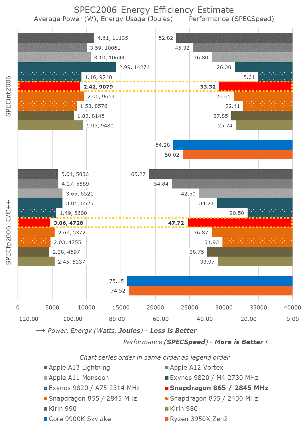
imho, if there is an ALU increase it will be 8 ALUs. Not 6 or 10. This is for the constrained aspect of the potential SMT4. When all threads are full they will only be able to 2 ALUs/2 FPUs at a given # of cycles, with a restricted amount of registers usable for each thread. With that increase the FPU vALUs will also increase from 4 FP256 vALUs to 8 FP128 vALUs. Which is already physically implemented in the Zen2 design. The only thing left is the promised core refactorization.
The SMT4 allows for:
- a reduction of amount of cores used, which benefits single(eighth die)-two(quarter die)-quad core(half die) boosts.
- increased utilization of units at high frequency, better ILP/EPI at 3~5 GHz.
Maybe...
4x28 instead with simpler ALUs having integrated LD/ST AGUs.
4x16 + 1x28 => 92-entry tSQ, 4x28 => 112-entry tSQ
5 SQs(7-units) to 4 SQs(8-units)
FPU side might have two separate FP128 four-issue SQs rather than a single FP256 four-issue SQ. If NSQ dispatches Lo-128(MUL0) or Lo-256(MUL0/MUL1) to SQ0, it also must dispatch Hi-128(MUL2) or Hi-256(MUL2/MUL3) to SQ1. If NSQ dispatches Lo-128(ADD0) or Lo-256(ADD0/ADD1) to SQ0, it also must dispatch Hi-128(ADD2) or Hi-256(ADD2/ADD3) to SQ1. NSQ can continue with 4-issue with lo-half first 4 and hi-half second 4, or they could target eight issue. The same applies to the 8 ALU design, four AGUs then four ALUs. If there is no hi-half then it is all lo-half, or if its all ALU or AGU, then there is no AGU or ALU ops dispatched.
6 units (4+2) => 192 -> 32x6 (Maximum of 6 micro-op)
7 units (4+3) => 224 -> 32x7 (Maximum of 7 micro-op)
8 units(4 Complex + 4 Simple/AGU) => 256? -> 32x8, if AMD wants to be on-par with Sunnycove this will have to be 44x8 => 352 retire. (Maximum of 8 micro-op) <== Refactored with FPU (8 INT or 8 FP)
Last edited:


