Discussion Optane Client product current and future

Page 21 - Seeking answers? Join the AnandTech community: where nearly half-a-million members share solutions and discuss the latest tech.

IntelUser2000

Elite Member
Oct 14, 2003
8,686
3,785
136
Channels are the limiting factor.....but there also needs to be enough Gen 1 dies to fill the 300 MB/s capacity of each channel.

No, they talked about this during Optane launches. I don't know why you are suddenly changing altogether. NAND needs multiple dies to saturate channel because the media is slow. 3D XPoint's write-in-place media and inherently faster chip negates that. It's same with DDR. You can get per DIMM bandwidth figures by multiplying the width per IC times the speed(in MT/s) the IC is running at. No needing to saturate or anything like that.

A single NAND flash die isn't enough to keep one of the controller's channels busy, because flash takes many microseconds to complete a read or write command, and even longer for erase commands. By contrast, 3D XPoint memory is fast enough that there is little to no performance to be gained from overlapping commands to multiple dies on a single channel

Bandwidth is determined by the internal connections to the IC. The manufacturer determines how wide and how fast it can be. So if they want 16GB Optane to be having 1GB/s it can. Why it runs at such speed and how wide it is only the engineers at Intel knows.
 

cbn

Lifer
Mar 27, 2009
12,968
221
106
NAND needs multiple dies to saturate channel because the media is slow. 3D XPoint's write-in-place media and inherently faster chip negates that.

Not for Sequential write.

The current Optane media is too slow per die in that category.
 

IntelUser2000

Elite Member
Oct 14, 2003
8,686
3,785
136
Not for Sequential write.

The current Optane media is too slow per die in that category.

Oh boy, I don't know if you are doing this in purpose or not.

It may be limited in the DIMM variants where the latency is in the nanoseconds, but clearly not in the SSD space where its in double digit microseconds. If it was that slow, then Optane wouldn't be able to imagine being in a DIMM form factor at all.

Anandtech article tells you otherwise.
 

cbn

Lifer
Mar 27, 2009
12,968
221
106
So why is the 16GB Optane not able to over 150 MB/s Sequential write? (This despite the original optane memory 16GB having the same 3.5W active power as the 32GB Original Optane memory).

And why is it that each Optane die added adds another 150 MB/s?

It seems to me In order to get 300 MB/s Sequential write per die (@ 20nm lithography) Intel is going to need 4 layer dies (with the same parallelness per layer as Gen 1).

P.S. I understand how each Optane die would be faster in a DIMM, but we have talking about NVMe Optane.
 
Last edited:

IntelUser2000

Elite Member
Oct 14, 2003
8,686
3,785
136
(Any harshness directed I apologize)

Yes, we don't know the details for SSDs as we do for CPUs or DRAM. But for DRAM, each IC runs at a certain speed(Megatransfers, or MT/s, similar to MHz) and has certain bit width.

Optane on 900P may be running at twice the frequency to achieve twice the bandwidth. It can afford to do so.

The M10 can boast much improved perf/watt not just due to binning but due to having active power management, because TDP is basically "typical worst case" and power management can reduce number of code from reaching TDP. That means, it might throttle in a few.

This is just a guess, but due to defects the original controller may have been limited to 2 channels, and had disabled power management. Also, multi-die packaging may not have been ready and simply just used 2 channels.
 
Last edited:

cbn

Lifer
Mar 27, 2009
12,968
221
106
Remember how you were talking about using even smaller capacities(maybe 8GB?) to get more channels thus more bandwidth? If its power limited then you won't get much higher bandwidth.

I did speculate on IMFT using a small (+ medium and large) die strategy for Gen 2 in the same way IMFT did with Gen 2 NAND.

So instead of 4 layer 256Gb (32GB) Gen 2 dies @ 300 MB/s write per die (for NVMe) the smallest die would be 4 layer 64Gb (8GB) Gen 2 dies at 300 MB/s write (for NVMe) and the mid size would be 4 layer 128Gb (16GB) Gen 2 dies at 300 MB/s write (for NVMe)

Now if that happened you would need more channels per GB and power consumption per GB would increase but so would performance per GB.
 
Last edited:

IntelUser2000

Elite Member
Oct 14, 2003
8,686
3,785
136
If true, then I would imagine a 64GB Gen 2 Optane using about as much power as a hypothetical 256GB Gen 1 Optane. (The closest I can think of would be the 380GB 900p M.2 at 9.5W active power-->

I think we can do better, and that's what M15 will show.

And:

Optane H10
-2600MB/s Read, 2000MB/s write
-Greater than 300TBW endurance

They are "up to figures". I'm guessing the random read figures will be worse than Optane but better than NAND. It's promising and I may be hoping too much from it!
 

cbn

Lifer
Mar 27, 2009
12,968
221
106
Optane H10
-2600MB/s Read, 2000MB/s write
-Greater than 300TBW endurance

They are "up to figures". I'm guessing the random read figures will be worse than Optane but better than NAND. It's promising and I may be hoping too much from it!

So H10 does not have PCIe x 2/PCie x 2 configuration!

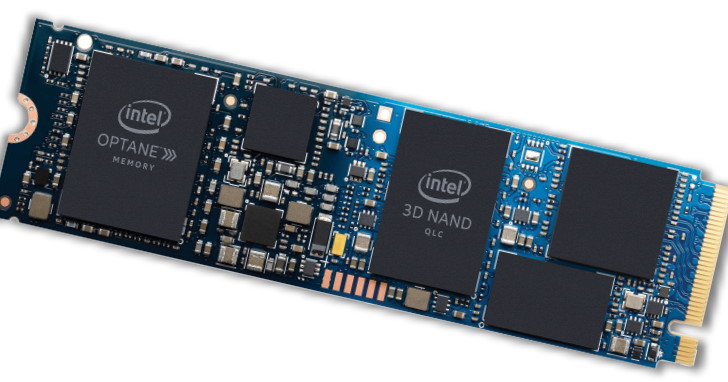
And I'll bet it looks different than this picture:

75cdab576c53822967661cd413ba4dec.jpg


My guess Optane controller package is larger, but Optane die package is smaller.
 

IntelUser2000

Elite Member
Oct 14, 2003
8,686
3,785
136
My guess Optane controller package is larger, but Optane die package is smaller.

It might be, but I can't say for sure. The video from PCWorld shows the module, and it looks same as the picture, so it seems to be an accurate one.

It's definitely something different.

Update: A Chinese translation of a site says the Optane portion of H10 is not directly accessible to the user. And it will not be able to be able to accelerate HDDs if installed, so its for the on board SSD. It makes sense.


Lenovo product leak shows Optane H10(Teton Glacier) for the T490s. That's based on Whiskey Lake though.
 
Last edited:
  • Like
Reactions: Dayman1225

cbn

Lifer
Mar 27, 2009
12,968
221
106
Looking at the following slide:

intel-ssd-optane-h10-slajd.jpg


It does say PCIe Gen 3.0 x4 (2x2) in the lower left hand corner.

So in order to get 2600 MB/s read and 2000 MB/s write the Optane and the QLC NAND must be working together in an additive fashion.

The only thing I can think of that would be reliable enough would be what nosirrahx described here:

https://forums.anandtech.com/thread...-price-and-performance.2552818/#post-39543663

But how about the writes?

Is writing a file from opposite ends (on cache and backing store) actually more reliable than write back? The way I am imagining it I think it would be.
 
Last edited:

IntelUser2000

Elite Member
Oct 14, 2003
8,686
3,785
136
It does say PCIe Gen 3.0 x4 (2x2) in the lower left hand corner.

Regardless of what they are doing, that benchmark is further indication that sequentials are much faster than Optane Memory. It won't beat the 970 Pro that much without fast enough sequentials.
 

nosirrahx

Senior member
Mar 24, 2018
304
75
101
Looking at the following slide:

So in order to get 2600 MB/s read and 2000 MB/s write the Optane and the QLC NAND must be working together in an additive fashion.

The only thing I can think of that would be reliable enough would be what nosirrahx described here:

https://forums.anandtech.com/thread...-price-and-performance.2552818/#post-39543663

If I was on this project, this is certainly how I would implement the caching technology.

If Intel is doing this they should come up with a buzz-word for the new technology like RIAD C (C for cache). This would essentially be a hybrid of RAID 0 and RAID 1 on a single drive with 2 banks, 1 of them being much smaller but faster than the other.
 

cbn

Lifer
Mar 27, 2009
12,968
221
106
Optane on 900P may be running at twice the frequency to achieve twice the bandwidth. It can afford to do so.

According to Intel Ark 280GB 900p has 14W active power and 5W idle.

https://ark.intel.com/content/www/u...-280gb-1-2-height-pcie-x4-20nm-3d-xpoint.html

This compared to Optane memory 16GB which has 3.5W active power and 1W idle.

https://ark.intel.com/content/www/u...es-16gb-m-2-80mm-pcie-3-0-20nm-3d-xpoint.html

(Compared to Optane memory 16GB the 900p 280GB has less power available per channel...with the idle on 900p being pretty high too.)
 

IntelUser2000

Elite Member
Oct 14, 2003
8,686
3,785
136
They are not directly comparable. You can see with the 905P, the M.2 version has lower active and idle power than non-M.2 devices 900P/905P also don't have power management. There are too many variables to simply divide watts by channels.

You can see the impact of bandwidth and power with the P4801X: https://ark.intel.com/content/www/us/en/ark/compare.html?productIds=149367,149365,149364,149366

The data center products have higher TDP because they are less bursty than client and set to higher TDP to minimize throttling.

(I wish reviewers tested various capacities rather than just assuming they all perform the same)
 
Last edited:

cbn

Lifer
Mar 27, 2009
12,968
221
106
They are not directly comparable. You can see with the 905P, the M.2 version has lower active and idle power than non-M.2 devices 900P/905P also don't have power management. There are too many variables to simply divide watts by channels.

You can see the impact of bandwidth and power with the P4801X: https://ark.intel.com/content/www/us/en/ark/compare.html?productIds=149367,149365,149364,149366

The data center products have higher TDP because they are less bursty than client and set to higher TDP to minimize throttling.

(I wish reviewers tested various capacities rather than just assuming they all perform the same)

The two 100GB P4801X have 7 dies on 7 channels (with 7W TDP and 3W idle) but the write is only 1000 MB/s write. (So 142 MB/s per die).

Its only when moving up the 200GB P4801X does write improve to 2000 MB/s (It does have double the parallelism of the 100GB P4801X)
 

IntelUser2000

Elite Member
Oct 14, 2003
8,686
3,785
136
The two 100GB P4801X have 7 dies on 7 channels (with 7W TDP and 3W idle) but the write is only 1000 MB/s write. (So 142 MB/s per die).

I doubt this, and its using a combination of lower clocks and lower number of channels(die harvesting on the controller). After all, they are called Low Power Optane.
 

cbn

Lifer
Mar 27, 2009
12,968
221
106
I doubt this, and its using a combination of lower clocks and lower number of channels(die harvesting on the controller). After all, they are called Low Power Optane.

Anandtech says the 100GB P4801X still uses the full seven channel controller:

https://www.anandtech.com/show/13387/intel-expands-optane-905-ssds-to-15tb

On the enterprise side of things, the P4801X M.2 drive has still not officially launched, but ark.intel.com is listing a 100GB P4801X U.2 drive. The capacity is similar to the Optane SSD 800P's 118GB limit, but the P4801X is still using the full seven-channel controller with a PCIe x4 host interface so performance is far higher.
 
Last edited:

IntelUser2000

Elite Member
Oct 14, 2003
8,686
3,785
136
Anandtech says the 100GB P4801X still uses the full seven channel controller:

I'm going to take it to mean the controller in its variation supports 7-channels. Whatever they are saying conflicts with their original claim that Optane doesn't need multiple chips per channel to maximize throughput. They are either wrong on the original claim, or the latest one. I'm going to go with the original claim since it makes more sense(because the 3D XPoint media compared to NVMe is many, many times faster and a single die per channel is enough to saturate it).

Since I cannot find the pictures of the P4801X products aside from the initial unveiling(which consisted of only 375GB part), I'll hold judgement.

You'll see that you'll have a very difficult time even finding the reviews for the 16GB variant of Optane Memory, even though it was released 2 years ago. Information on Optane in general are pretty sparse.
 
Last edited:

cbn

Lifer
Mar 27, 2009
12,968
221
106
Whatever they are saying conflicts with their original claim that Optane doesn't need multiple chips per channel to maximize throughput. They are either wrong on the original claim, or the latest one. I'm going to go with the original claim since it makes more sense(because the 3D XPoint media compared to NVMe is many, many times faster and a single die per channel is enough to saturate it).

Here is what the first Anandtech 900p review said:

https://www.anandtech.com/show/11953/the-intel-optane-ssd-900p-review/3

The Optane SSD 900P accesses its 3D XPoint memory more directly and read and write operations are completed synchronously without an intermediate buffering stage. This means that the 280GB and 480GB models have essentially the same performance, and this same level of performance could in theory extend down to a one die per channel configuration that would offer 112GB raw capacity and 96GB usable capacity (and could be profitably sold for under $180).

....But no Gen 1 Optane products that can do this that we know of so far.

With this noted, maybe Optane M15 uses Gen 1 dies and thus at 64GB and 1000 MB/s it becomes the first Gen 1 die Optane to break 160 MB/s write (per die).
 
Last edited:

cbn

Lifer
Mar 27, 2009
12,968
221
106
Regarding the Lenovo Teton Glacier leak:


One thing I noticed looking through that information is that any Lenovo laptop that needed a 2TB SSD (e.g. X1 Carbon G7) did not have Optane H10 (of any capacity) as an option.

But after doing the work I mentioned in this post I am convinced IMFT 96L 1536Gb 3D TLC die currently exists. That means IMFT 96L 2048Gb 3D QLC is probably right around the corner. (reason: 2048 Gb QLC is made from 1536 Gb TLC dies).

IMFT 96L 2048 Gb 3D QLC would allow Intel to hit 2TB NAND capacity with only one eight die package. (And therefore I imagine a 2TB Optane H10 is not that far away)
 

IntelUser2000

Elite Member
Oct 14, 2003
8,686
3,785
136
I just noticed there's more than one mention of H10, and some others talking about Optane in that leak. I only caught sight of one until now.

I am going to guess Optane next to DRAM section means "Optane Memory" and is a continuation of a sort of sleazy marketing practice. Unless they surprise us, and I'm not confident we'll see it so early.

Not sure about the Optane SSD part. It doesn't sound like H10, considering its mentioned in more than one place. 815P possibly? I assume 800P's adoption is very, very low, even by Optane standards and 815P usage would be a surprise.

One thing I noticed looking through that information is that any Lenovo laptop that needed a 2TB SSD (e.g. X1 Carbon G7) did not have Optane H10 (of any capacity) as an option.

This isn't anything more than Lenovo dipping their toe in the waters to see how customers and the market will react. And H10 is a very different product. If it works out, the successors might feature it more prominently.
 

nosirrahx

Senior member
Mar 24, 2018
304
75
101
This isn't anything more than Lenovo dipping their toe in the waters to see how customers and the market will react. And H10 is a very different product. If it works out, the successors might feature it more prominently.

I would not buy any Lenovo product with Optane. My experience so far has been that they lock the BIOS to specific parts so you cannot upgrade.

In my Asus Vivobook Pro I can use anything from the 16GB all the way up to the 118GB 800P and enable Optane without issue. The Lenovo Laptop I tried was BIOS locked to the 16GB module, even the 32GB module would fail to enable caching.

Vendors that intentionally cripple upgrade paths do not deserve consideration.
 

IntelUser2000

Elite Member
Oct 14, 2003
8,686
3,785
136

VirtualLarry

No Lifer
Aug 25, 2001
56,327
10,035
126
Wow, that IS Big News, Intel relents on some of their obscene levels of product segmentation, and allows usage of Optane Memory (caching) support on Celerons and Pentiums? (8th-Gen only, apparently, and must be supported by the mobo vendor by a BIOS update?)

Sounds good to me, I agree, a step in the right direction.

Edit: Quick Q, what chipset level do you need for Optane Memory support for 8th-Gen Core/Celeron/Pentium? Will all Intel 8th-Gen capable mobos with an NVMe slot that supports Optane do it? Or is there a chipset-level limitation too?

Looking to do an Optane test build, to get my feet wet, probably next month. (Also want to do an A300W DeskMini build, but that's OT for this thread.)

Edit: What's the best/cheapest config for Optane? 32GB Optane Memory + 4TB-6TB HDD? Or 32GB Optane Memory + 1TB Samsung 860 QVO SATA6G 2.5" SSD? Or would getting an Intel 660p 1TB-2TB M.2 NVMe be better, and skip the Optane? Or even use an Optane, with the 660p, as a cache? Would it even make sense to cache NVMe with another NVMe?

Or, what about these new Optane + QLC M.2 NVMe combo SSDs? Are they going to be "transparent" about the caching, like Seagate Firecuda SSHDs, or like the WD Black^2, that acted like two devices, as I understand it?

Thinking in terms of an A300 DeskMini, with an Athlon 200GE in it, which only has x2 lanes for the NVMe bonded out, and if the initial Hybrid Optane / QLC drives, require PCI-E bifurcation support, for twin x2 devices on the same PCB, those won't work with the A200GE then.
 
Last edited: