Discussion Leading Edge Foundry Node advances (TSMC, Samsung Foundry, Intel)

Page 114 - Seeking answers? Join the AnandTech community: where nearly half-a-million members share solutions and discuss the latest tech.

DisEnchantment

Golden Member
Mar 3, 2017
1,614
5,849
136
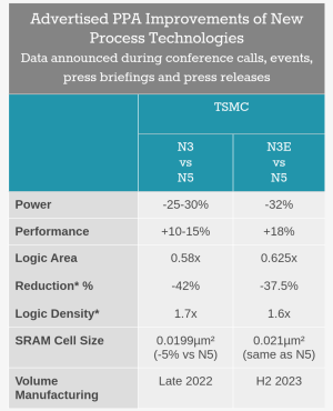
TSMC's N7 EUV is now in its second year of production and N5 is contributing to revenue for TSMC this quarter. N3 is scheduled for 2022 and I believe they have a good chance to reach that target.

1587737990547.png
N7 performance is more or less understood.
1587739093721.png

This year and next year TSMC is mainly increasing capacity to meet demands.

For Samsung the nodes are basically the same from 7LPP to 4 LPE, they just add incremental scaling boosters while the bulk of the tech is the same.

Samsung is already shipping 7LPP and will ship 6LPP in H2. Hopefully they fix any issues if at all.
They have two more intermediate nodes in between before going to 3GAE, most likely 5LPE will ship next year but for 4LPE it will probably be back to back with 3GAA since 3GAA is a parallel development with 7LPP enhancements.

1587739615344.png

Samsung's 3GAA will go for HVM in 2022 most likely, similar timeframe to TSMC's N3.
There are major differences in how the transistor will be fabricated due to the GAA but density for sure Samsung will be behind N3.
But there might be advantages for Samsung with regards to power and performance, so it may be better suited for some applications.
But for now we don't know how much of this is true and we can only rely on the marketing material.

This year there should be a lot more available wafers due to lack of demand from Smartphone vendors and increased capacity from TSMC and Samsung.
Lots of SoCs which dont need to be top end will be fabbed with N7 or 7LPP/6LPP instead of N5, so there will be lots of wafers around.

Most of the current 7nm designs are far from the advertized density from TSMC and Samsung. There is still potential for density increase compared to currently shipping products.
N5 is going to be the leading foundry node for the next couple of years.

For a lot of fabless companies out there, the processes and capacity available are quite good.
 

H433x0n

Senior member
Mar 15, 2023
898
968
96
Intel to use direct self assembly + high-NA euv for 14A process: https://www.semianalysis.com/p/intels-14a-magic-bullet-directed
Apparently this is why Intel is buying all these high NA tools. According to the link, Intel could scale M0 metal pitch all the way to ~20nm, which seems again very aggressive (down from 36nm in 18A). If other structures scale accordingly, this could result in large density increase... Let's hope they don't repeat 10nm fiasco. Imo, a much less risky approach would be to use DSA + low-NA EUV tool (M0 could still come down to ~30nm + they could use the same tools as for Intel 3 and 18A).
18A MMP is not 36nm. That was an Intel 4 test chip with BPD. The vanilla Intel 4 node has an MMP of 30nm.

If I had to guess 18A MMP is 26-28nm depending on how aggressive they went. It’s certainly no more than 30nm.
 

Doug S

Platinum Member
Feb 8, 2020
2,281
3,540
136
From TSMC call. It seems Apple is not the first customer on N2 this time.

We all knew that from the timing of when N2 comes out. The open question is at what volume will N2 be produced when it enters mass production. Remember N3B's "mass production"?

Maybe all the big players wait for the "real" N2 six months later that includes BSPDN, in which case the N2 rollout looks like the N3B rollout where it sees little apparent use (we still haven't heard of anyone shipping N3B silicon other than Apple, it was probably cryptominers and the like) until Apple delivers the real volume later in 2026.
 

Ghostsonplanets

Senior member
Mar 1, 2024
321
489
96
Maybe all the big players wait for the "real" N2 six months later that includes BSPDN, in which case the N2 rollout looks like the N3B rollout where it sees little apparent use
N2 does seems more of a transitory node until N2 BSPDN and N2P are ready. So that would make sense
we still haven't heard of anyone shipping N3B silicon other than Apple
Intel?
 

Doug S

Platinum Member
Feb 8, 2020
2,281
3,540
136

Unless I'm mistaken they haven't shipped anything with N3 content yet. And it remains to be seen if they are N3B or N3E. It would be frankly bizarre for them to use N3B for a product that isn't released until N3E is in mass production. Yeah yeah they could have done the designs long ago and were delayed, but at Intel's scale the savings and performance improvements would be worth it to redo it for N3E.
 

Ghostsonplanets

Senior member
Mar 1, 2024
321
489
96
Wait a second, who told you that? I wasn't aware that was rumoured already.

(Please don't take this as a confirmation of a leak or something like that, I've just not seen anyone say that on Twitter or anywhere else is all).
TDevilfish was the one who said it, late last year:

Unless I'm mistaken they haven't shipped anything with N3 content yet. And it remains to be seen if they are N3B or N3E. It would be frankly bizarre for them to use N3B for a product that isn't released until N3E is in mass production. Yeah yeah they could have done the designs long ago and were delayed, but at Intel's scale the savings and performance improvements would be worth it to redo it for N3E.
I had swear that a leak had it showing N3B as the node of choice, but I was wrong, so it's all speculation. Fair enough.
 
Last edited:

Doug S

Platinum Member
Feb 8, 2020
2,281
3,540
136
I had swear that a leak had it showing N3B as the node of choice, but I was wrong, so it's all speculation. Fair enough.

Oh I've seen those leaks that showing N3B, but I'm skeptical given the timeframe - and given TSMC's likely desire to avoid having one customer on N3B who can't begin to fill a single line's worth of output. That just creates misallocation of resources so it might have been worth it for TSMC to help with any costs Intel incurred porting to N3E.

Maybe the leaks are right and it will be N3B. Sometimes things happen that make no logical sense because of delays, stubbornness or stupidity.
 

Tigerick

Senior member
Apr 1, 2022
667
542
106
Personal attacks are not permitted here. Attack the post not the poster. It's the first rule of fight club/CPU forum.
Oh I've seen those leaks that showing N3B, but I'm skeptical given the timeframe - and given TSMC's likely desire to avoid having one customer on N3B who can't begin to fill a single line's worth of output. That just creates misallocation of resources so it might have been worth it for TSMC to help with any costs Intel incurred porting to N3E.

Maybe the leaks are right and it will be N3B. Sometimes things happen that make no logical sense because of delays, stubbornness or stupidity.
No, it is your REDACTED to accept N3B is better suit for Apple and Intel's requirement. Even though I told you many times N3B is having highest density in which Apple shown with M3 Max and upcoming M4 Max.

Just like you don't want to believe LPDDR6 is a game changer, now Apple is going to reset whole Mac lineup with LPDDR6. And yet you still don't believe due to your ego. I am sorry to say it is your REDACTED cause all this.
 
Last edited by a moderator:

SiliconFly

Golden Member
Mar 10, 2023
1,052
538
96
Unless I'm mistaken they haven't shipped anything with N3 content yet. And it remains to be seen if they are N3B or N3E. It would be frankly bizarre for them to use N3B for a product that isn't released until N3E is in mass production. Yeah yeah they could have done the designs long ago and were delayed, but at Intel's scale the savings and performance improvements would be worth it to redo it for N3E.
I don't think it's even the cost. I think they can't afford anymore additional delays.

...it might have been worth it for TSMC to help with any costs Intel incurred porting to N3E..
It's not just the cost. Time to market is crucial (more so now for a company like intel).
 

FlameTail

Platinum Member
Dec 15, 2021
2,356
1,275
106
What happens at the fab level when TSMC introduces a P-node?

For example: N5 -> N5P.

N5P has same density as N5 but with improved performance. Does TSMC create a new production line to produce N5P chips? Or do they upgrade the existing N5 line to an N5P line?

How about when TSMC introduces a nodelet (Example: N5 -> N4)?
 

SiliconFly

Golden Member
Mar 10, 2023
1,052
538
96
Or do they upgrade the existing N5 line to an N5P line?
As long as they're taking new contracts or fulfilling existing ones for a given node, there's no upgrading. They're obligated to hit the volume they've already committed to in the agreed upon time frame. No backsies there.

But they can always stop onboarding new customers/products and stop renewing existing contracts. Although, the later is very seriously frowned upon and can seriously diminish their credibility. And once the node is fully free, they can upgrade (or whatever else they want).
 

Aapje

Golden Member
Mar 21, 2022
1,393
1,878
106
What happens at the fab level when TSMC introduces a P-node?

For example: N5 -> N5P.

N5P has same density as N5 but with improved performance. Does TSMC create a new production line to produce N5P chips? Or do they upgrade the existing N5 line to an N5P line?

How about when TSMC introduces a nodelet (Example: N5 -> N4)?

I think that it depends on what they have to do to create the P-node or the nodelet. It's not like they are telling us exactly what they do to achieve this.
 

Doug S

Platinum Member
Feb 8, 2020
2,281
3,540
136
No, it is your REDACTED to accept N3B is better suit for Apple and Intel's requirement. Even though I told you many times N3B is having highest density in which Apple shown with M3 Max and upcoming M4 Max.

Just like you don't want to believe LPDDR6 is a game changer, now Apple is going to reset whole Mac lineup with LPDDR6. And yet you still don't believe due to your ego. I am sorry to say it is your REDACTED cause all this.

Wow you're really emotional about this. If it turns out you're wrong are you going to pull the classic internet forum move of deleting your account then coming back on a new one so you don't have to endure the shame of being wrong? Just a warning, we'll know its you if you won't stop talking about LPDDR6 because no one else here gets emotional about memory standards.

Density is the ONLY advantage of N3B, it loses to N3E in performance, power, and price. Apple cares about those three things more than they care about density. They will happily accept a low single digit percentage larger die area in exchange for a faster, cheaper, and most importantly of all to them lower power chip. I can't understand why you refuse to see that. Apple simply does not care about die area the way you think they do. The Max die is not even half reticle sized, they can easily go larger especially when "larger" is like 10 mm^2, if that.

I'm even more mystified why you've hitched your whole existence here on LPDDR6. That's a really odd horse to ride into battle, and the existence of Samsung's LPDDR5X-10700 makes the difference between 5X and 6 much smaller than when you decided to start your own thread extolling the virtues of LPDDR6 hoping you could make someone, anyone, else care. DRAM OEMs could really drop a turd on your parade if they managed to goose 5X up to 12800 before LPDDR6's debut lol
 

Saylick

Diamond Member
Sep 10, 2012
3,188
6,461
136
What happens at the fab level when TSMC introduces a P-node?

For example: N5 -> N5P.

N5P has same density as N5 but with improved performance. Does TSMC create a new production line to produce N5P chips? Or do they upgrade the existing N5 line to an N5P line?

How about when TSMC introduces a nodelet (Example: N5 -> N4)?
My guess is that the P-node replaces the original node entirely since the P-node should be an overall improvement and is PDK compatible with the original node. Additionally, it's typically in TSMC's favor to encourage customers to use the P-node because there's cost benefits for TSMC, i.e. lower production cost, some of which they pass on to the customer.
 

FlameTail

Platinum Member
Dec 15, 2021
2,356
1,275
106
Density is the ONLY advantage of N3B, it loses to N3E in performance, power, and price. Apple cares about those three things more than they care about density.
indeed.
chrome_screenshot_1699623262095.png
I'm even more mystified why you've hitched your whole existence here on LPDDR6. That's a really odd horse to ride into battle
In contrast, I ride the Snapdragon X Elite horse, which is way cooler:cool:
, and the existence of Samsung's LPDDR5X-10700 makes the difference between 5X and 6 DRAM OEMs could if they managed to goose 5X up to 12800 before LPDDR6's debut lol
This is something that baffles me about the existence of LPDDR5X-10700. That is basically getting into LPDDR6 territory in terms of speeds.

Remember when LPDDR5 came to market 5 years ago? The first devices with LPDDR5 (such as Galaxy S20 series) used LPDDR5-5500. It was only the next year that they adopted the full speed LPDDR5-6400 with the Galaxy S21 series.

Considering that LPDDR6 is basically 2x the bandwidth of LPDDR5, I assumed the first devices with LPDDR6 will have it running at 11000 Mbps (2× 5500). But now, the existence of LPDDR5X-10700 muddies the waters.
 
  • Like
Reactions: Tlh97

SpudLobby

Senior member
May 18, 2022
584
366
96
Wow you're really emotional about this. If it turns out you're wrong are you going to pull the classic internet forum move of deleting your account then coming back on a new one so you don't have to endure the shame of being wrong? Just a warning, we'll know its you if you won't stop talking about LPDDR6 because no one else here gets emotional about memory standards.

Density is the ONLY advantage of N3B, it loses to N3E in performance, power, and price. Apple cares about those three things more than they care about density. They will happily accept a low single digit percentage larger die area in exchange for a faster, cheaper, and most importantly of all to them lower power chip. I can't understand why you refuse to see that. Apple simply does not care about die area the way you think they do. The Max die is not even half reticle sized, they can easily go larger especially when "larger" is like 10 mm^2, if that.
Yep. This is why I thought they’d convert to N3E as soon as they can. The die being lower power with better yields (the two are related depending on your metric of course) is just huge. I would bet even after the die size increase it’s a bit cheaper with better avg power.

I'm even more mystified why you've hitched your whole existence here on LPDDR6. That's a really odd horse to ride into battle, and the existence of Samsung's LPDDR5X-10700 makes the difference between 5X and 6 much smaller than when you decided to start your own thread extolling the virtues of LPDDR6 hoping you could make someone, anyone, else care. DRAM OEMs could really drop a turd on your parade if they managed to goose 5X up to 12800 before LPDDR6's debut lol
Yeah I don’t understand the LPDDR6 parading.

It IS going to be big, the architecture itself + new nodes coming will likely offer further power gains and densities, and like LPDDR6x should hit 15+ GT/S, but that’s a ways off.


But I mean, LPDDR5 is really good and Apple haven’t eevn adopted LPDDR5x yet or anything faster than 6400, which is telling.
 
  • Like
Reactions: Tlh97

SiliconFly

Golden Member
Mar 10, 2023
1,052
538
96
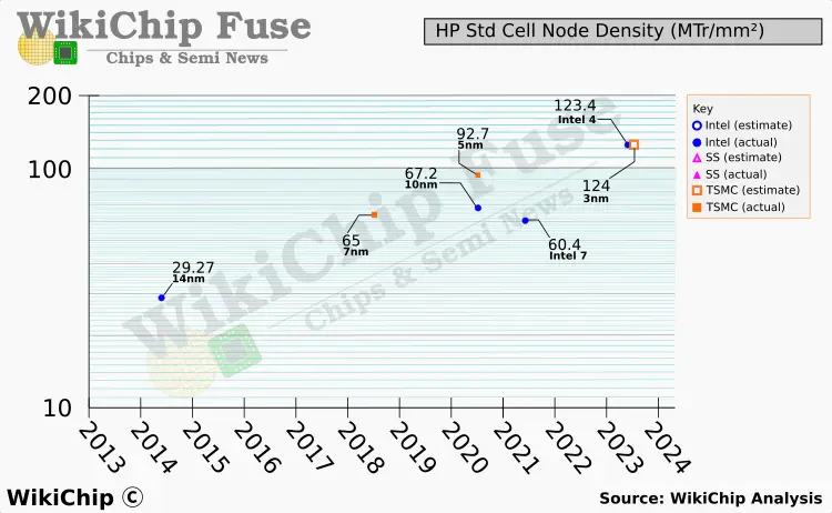
An interesting observation. Just came across this wikichip slide. Didn't notice properly at first. But upon closer look, just found it amazing.

https://fuse.wikichip.org/wp-content/uploads/2022/12/hp-density-14nm-5nm.png


Well, unlike others, this only squarely focuses on HP cell density only. If you look closely, you'll realize the HP cell density of TSMC N3 & Intel 4 are actually extremely close. Something I didn't notice before. Best part is, the relative sizes of HP & HD cells for any given node always tend to scale very similarly (for example, Intel 14, 7, TSMC N7, N5 & N3 all have very similar HP/HD scaling factor). Intel 4 doesn't have HD cells. But, this directly implies that, in theory, the HD cell density of Intel 4 & TSMC N3 are actually very close (even after accounting for any variations in cell sizes).

Now comes the interesting part, the upcoming N3E node is slightly more dense than the original N3. Same way, Intel 3 will be more dense than Intel 4 (I think around ~10% to 15%). This puts Intel 3 & N3E on the same ballpark.

Roughly around 215 million transistors/mm2 for both (+/- ~5). So, starting Q3 2024, its gonna be photo finish for either one of the nodes! Only a few more months. Thats exciting.

(Sadly, the first Intel 3 product is Sierra Forest based on the dated crestmont cores.) :(
 
Last edited: