Discussion Intel current and future Lakes & Rapids thread

Page 806 - Seeking answers? Join the AnandTech community: where nearly half-a-million members share solutions and discuss the latest tech.

Exist50

Platinum Member
Aug 18, 2016
2,452
3,106
136
Read again the point i was answering to.
I was adding on, not correcting.
Plus I'm not even sure of the timeline of when TSMC realized N3B was not yielding very well and decided to switch tracks to N3E, if N3E wasn't ever part of the original roadmap even.
There are three different nodes in play here. N3, N3B, and N3E. N3 was de facto canceled and replaced with (design compatible) N3B, though I'm not sure how exactly they differ. N3E is not design compatible. I think given Intel's typical timelines, N3B is the more realistic expectation, but that will disadvantage them against anything launching with N3E in a similar timeframe.
 

eek2121

Diamond Member
Aug 2, 2005
3,411
5,051
136
After all these years, Intel very badly needs a win. And to win, it need top-end high-performance parts like i9 & i7. No i5s and less.

Instead of making i9 & i7, meteor lake is restricted to low-end parts like i5 & i3. So, we have to conclude Intel 4 has yield issues (and/or maybe a bit of a clock regression).
As I said, Intel is limited by capacity. Intel 4 yields are actually very good, and no clock regression has been reported thus far.

Manufacturing an 8+16 die would have meant fewer dies overall.

My suspicion based on current info is that most of Intel’s EUV equipment is allocated elsewhere.

I do agree they need a win. Badly.

He again demonstrates he has no idea what he's talking about N3B and N3E are not design rule compatible, and no chance Intel's going to port it to both. I'd bet on N3B right now, but we'll see.

Per-core power regulation is also helpful for sparsely threaded loads. The low-frequency/idle cores don't have to be penalized by sharing the same voltage as the bursty ones.

I would almost bet money on Intel compute tiles not being made at TSMC for Arrow Lake. The only reason I don’t is because my information isn’t completely up to date.

Still, I believe it far more likely that AMD would start fabbing chips at an Intel fab than Intel fabbing their entire product at TSMC.

1) Fabbing the compute tiles at TSMC would destroy confidence in Intel fabs. Shares would tank and good luck selling IFS to others. (“you don’t even use your own fabs, why should we?”)

2) Margins would take a huge beating. Intel would have to pay a middle man to make their own chips.

The sources of the TSMC rumor are all folks with terrible track records.

Not one single “reliable” leaker has said Intel will be using TSMC.

I have been wrong before, but unless someone has a source that doesn’t involve a youtuber, I am going to continue to be super critical of this.
 

Geddagod

Golden Member
Dec 28, 2021
1,524
1,620
106
Also idk who wants to wants to go into so much effort as to fake this:
FMOhNpmWUAAV_WR.jpg:large
 
  • Like
Reactions: Tlh97 and Exist50

Abwx

Lifer
Apr 2, 2011
11,885
4,873
136
I was adding on, not correcting.

There was no need to add, i also adressed the point you re talking about at the begining of my sentence...

That being said they need one regulator per core, methink that this will be the case for the P cores while the e cores could use a single regulator for several cores, either one for 8 or for 4, that would greatly simplify the power management and provide a better reponsivness with little difference in perf/watt.
 

Geddagod

Golden Member
Dec 28, 2021
1,524
1,620
106
And also, I want to add if LNL is not using TSMC 3nm, then Pat saying it's launching 2024 is pretty much impossible. Since the two nodes for LNL and beyond were supposed to be Intel 18 and external fabs, and 18A products in 2024 is pretty much impossible, that just leaves an external node for LNL.
Plus, since LNL and ARL are supposed to use the same core arch, if LNL is on an external node, there's really no reason ARL couldn't be as well.
 

H433x0n

Golden Member
Mar 15, 2023
1,224
1,606
106
Also idk who wants to wants to go into so much effort as to fake this:
FMOhNpmWUAAV_WR.jpg:large
Isn't this a slide for a mobile product? That's the one that's rumored to be on 20A?

Also - Can somebody explain to me how it makes sense to make ARL on both N3 and 20A? These 2 nodes seemingly couldn't be more different. How are you going to carry over an arch with design rules for GAA and PowerVia and port it over to N3 without a significant time investment? This is ignoring it's 2 totally separate PDKs (one for TSMC FinFet, the other for IFS GAA). Looking at it from a high level, it doesn't make much sense.

Edit: From what I can tell, if they make Lion Cove on TSMC N3, you're committing quite a lot to it. It seems like there's 2 options if they decide to use TSMC N3 for ARL.

A) Building all of your compute tiles on TSMC for this generation.
B) Performing the work twice by porting it back to 18A once it's ready, which seems like it'd be quite a lengthy process and by the time you're done you're almost done with the arch anyway.
 
Last edited:

mikk

Diamond Member
May 15, 2012
4,296
2,382
136
And also, I want to add if LNL is not using TSMC 3nm, then Pat saying it's launching 2024 is pretty much impossible. Since the two nodes for LNL and beyond were supposed to be Intel 18 and external fabs, and 18A products in 2024 is pretty much impossible, that just leaves an external node for LNL.
Plus, since LNL and ARL are supposed to use the same core arch, if LNL is on an external node, there's really no reason ARL couldn't be as well.


Imho they confirmed it already with the slide from last year. Lunar Lake and external are on the left side. 18A and beyond on the right. 18A belongs to the successor of Lunar Lake. Kinda similar with Meteor Lake. We have Meteor Lake and Intel 4 on the left which belongs together. Also we have External N3 and Arrow Lake on the right, imho it belongs together. And 20A in the middle because Arrow uses both. GPU tiles are missing there, MTL uses 5nm.
 
  • Like
Reactions: Geddagod

Exist50

Platinum Member
Aug 18, 2016
2,452
3,106
136
There was no need to add, i also adressed the point you re talking about at the begining of my sentence...
You said nothing about per-core, or how well threaded a load is. Anyway, they're almost certainly using one DLVR per 4 core cluster. They already share the same clock domain, iirc.
Also - Can somebody explain to me how it makes sense to make ARL on both N3 and 20A? These 2 nodes seemingly couldn't be more different. How are you going to carry over an arch with design rules for GAA and PowerVia and port it over to N3 without a significant time investment?
They're just going to have to brute force it. It surely won't be easy or cheap, but things probably wouldn't have been much better if the split was Intel 3 and Intel 20A either. It wouldn't be surprising if we were to see a staggered launch between the N3 and 20A parts, however.
 

Geddagod

Golden Member
Dec 28, 2021
1,524
1,620
106
Imho they confirmed it already with the slide from last year. Lunar Lake and external are on the left side. 18A and beyond on the right. 18A belongs to the successor of Lunar Lake. Kinda similar with Meteor Lake. We have Meteor Lake and Intel 4 on the left which belongs together. Also we have External N3 and Arrow Lake on the right, imho it belongs together. And 20A in the middle because Arrow uses both. GPU tiles are missing there, MTL uses 5nm.
Huh that kind of makes sense.
Also if PTL uses 18A, I don't have much confidence it's going to be anything less than a node shrunk LNC coming in 2025 2H , but it's way too far in the future to speculate about prob
 

Geddagod

Golden Member
Dec 28, 2021
1,524
1,620
106
Isn't this a slide for a mobile product? That's the one that's rumored to be on 20A?

Also - Can somebody explain to me how it makes sense to make ARL on both N3 and 20A? These 2 nodes seemingly couldn't be more different. How are you going to carry over an arch with design rules for GAA and PowerVia and port it over to N3 without a significant time investment? This is ignoring it's 2 totally separate PDKs (one for TSMC FinFet, the other for IFS GAA). Looking at it from a high level, it doesn't make much sense.

Edit: From what I can tell, if they make Lion Cove on TSMC N3, you're committing quite a lot to it. It seems like there's 2 options if they decide to use TSMC N3 for ARL.

A) Building all of your compute tiles on TSMC for this generation.
B) Performing the work twice by porting it back to 18A once it's ready, which seems like it'd be quite a lengthy process and by the time you're done you're almost done with the arch anyway.
Ye, apparently Intel switched what segmentation they are going to use N3 and Intel 20A for. One has to wonder why, perhaps they want to use internal node for their high margin and more important lineup of mobile, perhaps TSMC 3nm just has higher fmax than Intel 20A, etc etc

Also if LNC uses two nodes, the ideal reality would be to develop them simultaneously. I don't think the core arch is as 'glued' to the process node as you think it is... specific implantation may help achieve better density or better performance in one variant or another, but I think it's still possible. And tbh, imo, LNC was originally meant for Intel 7nm/Intel 3, but got pushed onto 18A because Intel thought they would have that node ready by then, also because of additional delays elsewhere. But that's a whole other discussion.

When core archs are being developed, I'm assuming architects imagine their node, see what the density/power they could achieve with it, and then add additions to parts of the pipeline accordingly, making sure that they don't "blow up" the core area or have clocks and power consumption be impacted too heavily versus previous gen. IIRC Intel had a general rule of their new archs having a 1%:1% ratio of better perf/better power efficiency, though idk how much they still follow it or what happened to that rule.
 

DrMrLordX

Lifer
Apr 27, 2000
22,903
12,974
136
I was adding on, not correcting.

There are three different nodes in play here. N3, N3B, and N3E. N3 was de facto canceled and replaced with (design compatible) N3B, though I'm not sure how exactly they differ. N3E is not design compatible. I think given Intel's typical timelines, N3B is the more realistic expectation, but that will disadvantage them against anything launching with N3E in a similar timeframe.

N3/N3B aren't design-rule compatible with Intel 20a either. The only way Arrow Lake-S is on N3-anything is if Intel planned this well in advance, at least as a backup in case Intel 20a wasn't ready on time.
 

A///

Diamond Member
Feb 24, 2017
4,351
3,160
136
my own reasoning of why it makes no sense is if intel desrisked a future node by trying and successfully doing bpd now with intel 4 rather then later and expecting to slam out bpd designed within 2 years when tsmc will be coming in later with their take on bpd and samsung will be in the corner eating melted styrofoam. but let gedda pom his pom poms we all need something to waste our time on.
 
  • Haha
Reactions: igor_kavinski

moinmoin

Diamond Member
Jun 1, 2017
5,242
8,456
136
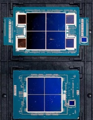
This is the first time I see these Side by Side. And yes the Compute tile on SPR-HBM is Larger.

View attachment 80427
So apparently the HBM version is sufficiently different that Intel said it's not worth the hassle applying the shrink they managed for the non-HBM tiles.

By using chiplets AMD managed to vastly reduce the amount of distinct dies they had to design for different markets. Intel somehow managed to achieve the exact opposite so far.
 

eek2121

Diamond Member
Aug 2, 2005
3,411
5,051
136
Also idk who wants to wants to go into so much effort as to fake this:
FMOhNpmWUAAV_WR.jpg:large
Where did the slide originate? The issue is that this slide could very likely be taken out of concept. This could simply be from an engineer proposing an alternate scenario in case of Intel fab issues, or it could be part of a slide deck providing all possible scenarios for discussion.

There is a reason it is marked “Not for External Communication“.

Companies I have worked at do similar slides when discussing the best path forward.

There is no way to know without context.
 

Geddagod

Golden Member
Dec 28, 2021
1,524
1,620
106
my own reasoning of why it makes no sense is if intel desrisked a future node by trying and successfully doing bpd now with intel 4 rather then later and expecting to slam out bpd designed within 2 years when tsmc will be coming in later with their take on bpd and samsung will be in the corner eating melted styrofoam. but let gedda pom his pom poms we all need something to waste our time on.
Let me get this straight. You don't believe LNC could be on TSMC 3nm... because it lacks BPD?
 

A///

Diamond Member
Feb 24, 2017
4,351
3,160
136
i don't believe in anything til i see it happen. too much bullshit with rumors now a days.

you're hear believing almost everything you see. you say who had time to fake a slide. fake slides have been a recurrance for years.
 

mikk

Diamond Member
May 15, 2012
4,296
2,382
136
Faked Intel slides are very rare. We don't get much leaked Intels slides nowadays anyways. It shouldn't surprise anyone when Lion Cove+Skymont is made with a TSMC node in some of the versions. Even if it's not ARL-S there is Lunar Lake which I think Intel confirmed the external process in the slide from last year. It's suspicious Intel never really mentioned an Intel process when they referred to Lunar Lake. They are happy to tell us Clearwater Forest is coming with 18A in 2025 but didn't tell anything specific about Lunar Lake.
 
  • Like
Reactions: Exist50
Jul 27, 2020
28,041
19,146
146
Maybe Lunar Lake is their first real wide scale test of TSMC's process tech for CPU chiplets. Going forward, they might keep mobile CPUs on TSMC and desktop CPUs on IFS.
 

Exist50

Platinum Member
Aug 18, 2016
2,452
3,106
136
So apparently the HBM version is sufficiently different that Intel said it's not worth the hassle applying the shrink they managed for the non-HBM tiles.

By using chiplets AMD managed to vastly reduce the amount of distinct dies they had to design for different markets. Intel somehow managed to achieve the exact opposite so far.
There's no way around it. The HBM version needs the memory controller/PHY that simply doesn't exist on the normal SPR die. So either you add a large chunk of silicon that 99% of your market can't even use, or you make another die.