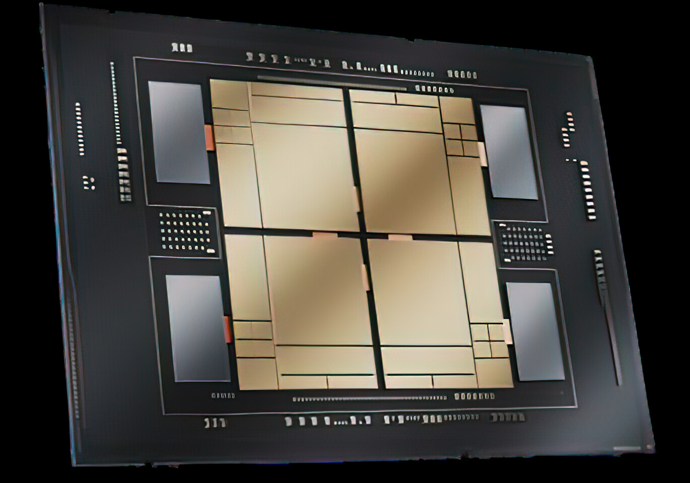
So they get 68 full sized dies out of the whole 300mm wafer. the partial dies are not functional and are discarded. Out of those 68 only 34-40 are still functional(some dies will have minor defects that will just be a lower tier CPUs with lower cores)
So let's say that Intel spends about $3,000 per wafer(As per Dr. Ian Cutress estimate of 1/3 cost for Intel as opposed to TSMC Cost of $10,000 per finished wafer), that would mean that each fully functional die is about $75-88 per piece. That is still not that much and Intel can just keep "Printing" more of them.
The issue would be how fast can they ramp up production?