Huh, that is actually very interesting and way awesome. So you obviously never want a CPU to fail, but that's pretty awesome that a core can fail, but the CPU will just disable that core and continue running. I haven't worked in IT for years, but that sounds like a pretty awesome feature to help keep servers running and find potential failures without the entire machine going down.If my understanding is correct, it would be something like if a core breaks, they can just disable that core and otherwise be fine. Though I will say that 76% seems kind of low if that's actually the metric. There's also definitely some degree of fault tolerance in there though. I think Apple goes hardest on that.
-
We’re currently investigating an issue related to the forum theme and styling that is impacting page layout and visual formatting. The problem has been identified, and we are actively working on a resolution. There is no impact to user data or functionality, this is strictly a front-end display issue. We’ll post an update once the fix has been deployed. Thanks for your patience while we get this sorted.
You are using an out of date browser. It may not display this or other websites correctly.
You should upgrade or use an alternative browser.
You should upgrade or use an alternative browser.
Discussion Intel current and future Lakes & Rapids thread
Page 609 - Seeking answers? Join the AnandTech community: where nearly half-a-million members share solutions and discuss the latest tech.
Oh I'm not talking about in a live system. This is all at manufacturing time. If you're looking for that degree of fault tolerance, however, I think IBM's mainframes might be capable of it. They can do some pretty crazy stuff.Huh, that is actually very interesting and way awesome. So you obviously never want a CPU to fail, but that's pretty awesome that a core can fail, but the CPU will just disable that core and continue running. I haven't worked in IT for years, but that sounds like a pretty awesome feature to help keep servers running and find potential failures without the entire machine going down.
Henry swagger
Senior member
When intel is shipping 4 million of dg2 their confident in there productLet's get two things clear people. Maybe you don't believe Intel, but you prefer to believe from AdoredTV? Bolded points will address the leaks from Intel and their presentations.
384EUs are from Intel drivers. Nothing is more of a leak than that. WCCFTech may have decent sources sometimes but their conclusions are less accurate. ARL 6x4x16 is pretty clear. So they'd use the abbreviation from Arrowlake but it's actually for DG2? How does that make any sense? All the speculations, guessing, and thinking stops the moment the company itself speaks.
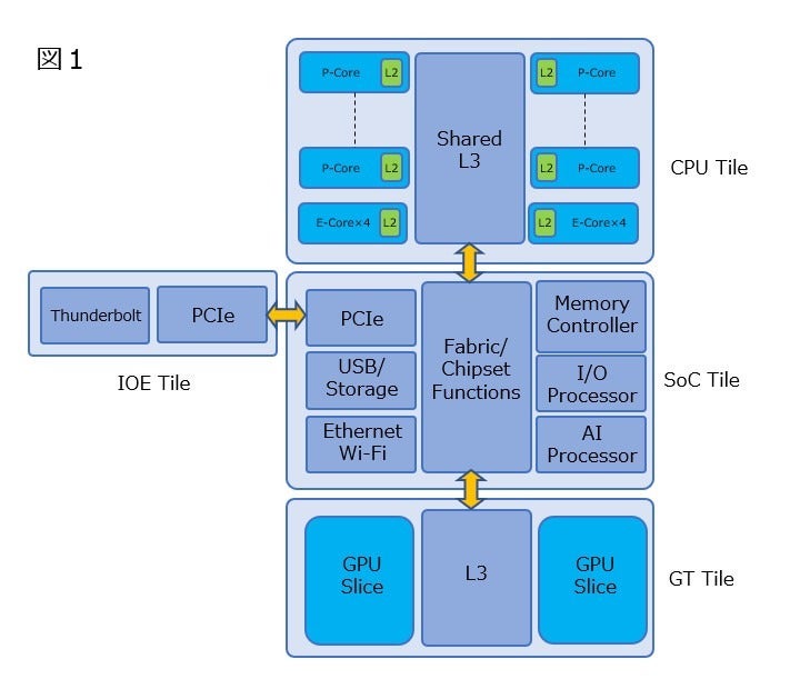
Meteorlake has I/O tile, Compute Tile, Graphics Tile, and SoC Tile. End of story. No need to argue about whether it makes sense to separate the SoC and I/O since they are doing it. And if they are using Foveros for Meteorlake, then it's pretty logical to conclude the Base is passive.
First, you are assuming that they haven't changed their plans. Looks like from the recent info they have ripped their roadmap apart and rebuilt it.
Second, we know already Xe is behind the state-of-the art from Nvidia and AMD. Nvidia beats the Xe with less compute and RDNA2 680M is pretty good, not to mention the old Vega 8 was pretty competitive with it.
So, while Xe could beat Vega 8 at 25W power envelopes, if we go below 20W Vega 8 pulls ahead.
Third, you are assuming Intel will perfect scaling up on the first try. They've never done it successfully before. Even the Skylake Iris Pro was pretty disappointing.
Meteorlake is a 2023-2024 part. H2 2023 might as well be a 2024 release, because it might spend more time in 2024 than in 2023. Where's the advantage of disaggregation if it takes the same time as before to bring new uarchs? Just stick to monolithic then.
Most of us expect DG2 is probably going to be perf/$ competitive. I'd challenge you to find a person that says the architecture in DG2 is on par with RDNA2 and Ampere.
If my understanding is correct, it would be something like if a core breaks, they can just disable that core and otherwise be fine. Though I will say that 76% seems kind of low if that's actually the metric. There's also definitely some degree of fault tolerance in there though. I think Apple goes hardest on that.
There are plenty of structures that don't lend themselves to redundancy, like everything that manages core to core communication, data buses between cores and external cache, memory and I/O controllers, etc.
74% seems pretty reasonable to me, just look at that die and everything marked MDF, DDR, PCIe, GPIO etc. on the edges is not redundant. Theoretically the DDR could be if e.g. they offered SKUs with fewer controllers, but in practice it would increase latency for the caches to support that so they probably require them all to be working. Maybe PCIe can be redundant if there are SKUs with fewer lanes. MDF definitely cannot.
You can definitely add redundancy on a circuit level to some degree. I think stuff like the memory controller and PHY is where that becomes problematic, because you want the highest possible speed/lowest delay. To what extent that's applicable here, I'm not sure.There are plenty of structures that don't lend themselves to redundancy, like everything that manages core to core communication, data buses between cores and external cache, memory and I/O controllers, etc.
74% seems pretty reasonable to me, just look at that die and everything marked MDF, DDR, PCIe, GPIO etc. on the edges is not redundant. Theoretically the DDR could be if e.g. they offered SKUs with fewer controllers, but in practice it would increase latency for the caches to support that so they probably require them all to be working. Maybe PCIe can be redundant if there are SKUs with fewer lanes. MDF definitely cannot.
oh, ok, my bad. I thought you were saying some consumer CPUs could do that currently or in the near future. That would be pretty cool! It'll arrive sometime 😀Oh I'm not talking about in a live system. This is all at manufacturing time. If you're looking for that degree of fault tolerance, however, I think IBM's mainframes might be capable of it. They can do some pretty crazy stuff.
moinmoin
Diamond Member
Schilling had a second post:
"Unused PCIe blocks in the south die are enabling I/O recovery through positional defeaturing. The Multi-Die Fabric IO (MDFIO) implements a lane repair to recover defects pre and post assembly. Test and debug solutions are implemented all over SPR."
Sounds a lot like scalable control fabric that Keller presumably introduced at AMD before for streamlining prototyping and die testing.
It's at the very least functionally duplicated to be redundant. Maybe it doesn't actually take twice the area, and the "extensive block repair/recovery methods" as well as "Thats mostly redundant circuits, but Intel is also talking about "extends techniques used"" are about reducing said duplication again without reducing redundancy.That’s a wrong conclusion. Something that can be recovered, doesn’t necessarily mean it’s duplicated.
You then go on about selling the chips with less cores. That's business as usual though, nothing new about that at all. If that process indeed features into the "74% recoverable dies" the whole message is essentially a smoke screen and the percentage is rather low as is even without above mentioned methods and techniques.I think that can be more accurately read as "What percentage of the die, if it breaks, still lets us sell a product".
That was funny, man! Keep going 🙂Tiger lake shipped 50 million units how are yields terrible ?
DrMrLordX
Lifer
When intel is shipping 4 million of dg2 their confident in there product
. . . what?
uzzi38
Platinum Member
Peanuts. That's not a large amount of product at all.When intel is shipping 4 million of dg2 their confident in there product
What's more, given the ASP of $75 (GPU + VRAM only), the overwhelming majority of DG2 that'll hit the market is the 128EU die.
That's not a confidence inspiring move.
First, you are assuming that they haven't changed their plans. Looks like from the recent info they have ripped their roadmap apart and rebuilt it.
What they have apparently changed or might have changed is the process node on some of their upcoming generations. Beside this what did they rebuilt? Changing a process node and architecture are two different things.
Arrow Lake or Lunar Lake was supposed to use TSMC 3nm entirely and now it's only the GPU tile apparently whereas CPU tile stays on Intel process node. Regarding Gen12.7/Xe HPG(or LPG) it's pretty clear from the driver and github sources. The last test driver was fairly new, it was build in December.
If you disagree with Intel sources you need a good source, saying you have to assume they haven't changed it isn't going to work. You are the one who told Looks like they changed the Meteorlake graphics architecture from DG2 based to Battlemage DG3 based.......so where do you see DG3 in Meteor Lake? I see zero sources or hints it could use a Battlemage based GPU.
You have to consider also that iGPUs are usually at least 1 year behind dGPU release schedules, just have a look to AMD in previous years. I think using Battlemage architecture for MTL would have been risky, there no guarantee Battlemage dGPU is release ready by mid 2023 and in fact ARL is a doubled MTL tile on the same architecture, this is what the driver says.
Nvidia beats the Xe with less compute and RDNA2 680M is pretty good, not to mention the old Vega 8 was pretty competitive with it.
This is based on the Xe LP architecture which is not used by Meteor Lake. It's using Gen12 HPG with higher IPC and a much better frequency scaling. Yes it's unclear by how much until we have real tests but using a graphics version not used by Meteor Lake to prove your point is silly, you can't prove it yet.
dullard
Elite Member
I'm curious as to how you went from:Meteorlake is a 2023-2024 part. H2 2023 might as well be a 2024 release, because it might spend more time in 2024 than in 2023. Where's the advantage of disaggregation if it takes the same time as before to bring new uarchs? Just stick to monolithic then.
- "powering on in Q2’22, shipping in 2023" https://download.intel.com/newsroom/2022/corporate/2022-Intel-Investor-Meeting-Client.pdf
- "2022 Milestones...Meteor Lake CPU tile production stepping tape out" https://download.intel.com/newsroom/2022/corporate/2022-Intel-Investor-Meeting-CEO.pdf
- every rumor along the lines of "2022 H2 ramp 2023 H1 products" https://www.anandtech.com/show/1682...nm-3nm-20a-18a-packaging-foundry-emib-foveros
- and when the rumors are more specific, they say Q2 2023: https://videocardz.com/newz/intel-14th-gen-core-meteor-lake-mobile-test-cpu-has-been-pictured
IntelUser2000
Elite Member
I'm curious as to how you went from:
to "might as well be a 2024 release".
Q2 might happen for the 5W M, because it doesn't exist, however with Raptorlake coming in late Q3 and Q4 it's unlikely they'll release majority of Meteorlake before that.
3 months in 2023 means 9 months in 2024. It's more of a 2024 product. And laptops we know takes 2-3 additional months to get it into consumer hands.
Peanuts. That's not a large amount of product at all.
What's more, given the ASP of $75 (GPU + VRAM only), the overwhelming majority of DG2 that'll hit the market is the 128EU die.
That's not a confidence inspiring move.
4 million+ would have been decent since it's pretty much just 9 months rather than 12 and it's their first year. Problem is according to the ASP it's dominated by sales of ultra low end dies similar to DG1.
This is worse than expecting that most would be laptop dies, since that could have been something like 3050 Ti mobile level. Instead it looks like it's MX450 class.
Arrow Lake-P was supposed to be the lead vehicle for TSMC 3nm:
dullard
Elite Member
If Apple is supposedly willing to pay for it, why would it be insane to produce?The idea that Intel would use N3 for the IGP, esp 80 mm2 is completely insane.
Arrow Lake-P was supposed to be the lead vehicle for TSMC 3nm:
And by the way
introduces LNC+SKT on N3
LNC= Lion Cove
SKT= Skymont
The old reddit leak was right once again.
dullard
Elite Member
I'm new to trying to decipher the lingo. Is 6C+8A referring to 6 Performance cores and 8 Efficiency cores or is it referring to 6 Performance and 8 clusters of 4 Efficiency cores (32 E cores total)?Arrow Lake-P was supposed to be the lead vehicle for TSMC 3nm:
It looks like Intel wanted more than 320 EUs (probably 384 EUs), couldn't fit more than 320 EUs into TSMC's requests, and if they scrap TSMC then they can go back to 384 EUs. Is that how you interpret it?
Intel annual gross profit ~$40B. Apple annual gross profit ~$160B.If Apple is supposedly willing to pay for it, why would it be insane to produce?
Apple has a little bit of wiggle room (plus absolute insane amounts of cash on hand).
I'm new to trying to decipher the lingo. Is 6C+8A referring to 6 Performance cores and 8 Efficiency cores or is it referring to 6 Performance and 8 clusters of 4 Efficiency cores (32 E cores total)?
It looks like Intel wanted more than 320 EUs (probably 384 EUs), couldn't fit more than 320 EUs into TSMC's requests, and if they scrap TSMC then they can go back to 384 EUs. Is that how you interpret it?
I don't know what 8A means, the reddit leak said ARL features a compute tile with 8/32 config for the high end enthusiast products which refers to ARL-S I have to assume, although 6+32 could make sense for mobile because 6+8 is a low core count. Final GT3 definition was WIP in this roadmap, seems like they increased it from 320 to 384EUs anyways.
It looks like Intel wanted more than 320 EUs (probably 384 EUs), couldn't fit more than 320 EUs into TSMC's requests, and if they scrap TSMC then they can go back to 384 EUs. Is that how you interpret it?
384 might be what's physically on the chip but they are only intending to do max 320.
Wow, now that was a leak. Does Jim normally just drop stuff like that on Twitter?
C = Core = P-core = Performance-core
A = Atom = E-core = Efficiency-core
Intel also uses TSMC for discrete Thunderbolt controllers, so maybe, despite being on a different node, it was easier to maintain that block as a separate tile rather than integrating it into the SOC tile. Anyway, before I saw all this stuff, I made an image to demonstrate just how small that tile is by comparing it to the M1 Pro floorplan. The M1 Pro is on TSMC N5, but I increased the size of the red box a bit to account for the 6% optical shrink that Intel might be able to get with N4. And I realize Apple and Intel are using totally different IPs, but it gives you a sense of the scale at least—maybe three Thunderbolt 4 controllers plus a PCIe Gen4 x4 PHY would fit. But it wouldn't even accommodate a single 128-bit LPDDR5 interface.

C = Core = P-core = Performance-core
A = Atom = E-core = Efficiency-core
That little tile is even smaller than what I said originally. It's only 5.1 mm x 2.0 mm = 10.2 mm². I'm guessing you're right about shoreline though. Despite the diminutive size, it still adds 25% to what's available otherwise on that SOC tile. As the dashboard posted above indicates, Intel refers to this as the IOE or IO Extension tile. I also found this MTL block diagram from a post back in January:I think it's probably some combination of Thunderbolt and/or PCIe controllers + PHY. Maybe the IPU and PHY or something else imaging related.
As for why they'd put it on there, probably shoreline. Must be cramped in the main SOC die, and I'd hate to imagine what it would be like routing high speed IO under one of the active dies. Also, it could let them support different configs for different markets. P needs more PCIe, Thunderbolt, whatever? Well then just swap out that one die instead of the whole SOC.
As for the process, I'm thinking N6 or something similar. Curious whether they use internal or external for that.
Intel also uses TSMC for discrete Thunderbolt controllers, so maybe, despite being on a different node, it was easier to maintain that block as a separate tile rather than integrating it into the SOC tile. Anyway, before I saw all this stuff, I made an image to demonstrate just how small that tile is by comparing it to the M1 Pro floorplan. The M1 Pro is on TSMC N5, but I increased the size of the red box a bit to account for the 6% optical shrink that Intel might be able to get with N4. And I realize Apple and Intel are using totally different IPs, but it gives you a sense of the scale at least—maybe three Thunderbolt 4 controllers plus a PCIe Gen4 x4 PHY would fit. But it wouldn't even accommodate a single 128-bit LPDDR5 interface.
I think this is converging in the right direction. Something like 2 TB4 + 4 or 8 lanes of PCIe for the M segment, maybe? And then you could make it longer to add more for P? I could see that. Definitely wouldn't want DDR on there, even if it'd fit. Too many hops.Wow, now that was a leak. Does Jim normally just drop stuff like that on Twitter?
C = Core = P-core = Performance-core
A = Atom = E-core = Efficiency-core
That little tile is even smaller than what I said originally. It's only 5.1 mm x 2.0 mm = 10.2 mm². I'm guessing you're right about shoreline though. Despite the diminutive size, it still adds 25% to what's available otherwise on that SOC tile. As the dashboard posted above indicates, Intel refers to this as the IOE or IO Extension tile. I also found this MTL block diagram from a post back in January:
Intel also uses TSMC for discrete Thunderbolt controllers, so maybe, despite being on a different node, it was easier to maintain that block as a separate tile rather than integrating it into the SOC tile. Anyway, before I saw all this stuff, I made an image to demonstrate just how small that tile is by comparing it to the M1 Pro floorplan. The M1 Pro is on TSMC N5, but I increased the size of the red box a bit to account for the 6% optical shrink that Intel might be able to get with N4. And I realize Apple and Intel are using totally different IPs, but it gives you a sense of the scale at least—maybe three Thunderbolt 4 controllers plus a PCIe Gen4 x4 PHY would fit. But it wouldn't even accommodate a single 128-bit LPDDR5 interface.
View attachment 57774
Frenetic Pony
Senior member
The idea that Intel would use N3 for the IGP, esp 80 mm2 is completely insane.
Battery life is a major concern for the mobile consumer space. Advantages in node power usage could play a very large part here, especially as 80mm is a lot of space in N3 terms. Apple just showed high end IGPs can be a big selling point.
Unfortunately, Apple also showed pretty clearly that they were Intel's only customer that actually wanted to pay for high-end IGPs.Battery life is a major concern for the mobile consumer space. Advantages in node power usage could play a very large part here, especially as 80mm is a lot of space in N3 terms. Apple just showed high end IGPs can be a big selling point.
That was just a size comparison; I never expected Intel would put a memory interface on its own tile. And looking over that program again, it appears that MTL-M/P and ARL-P might share a common SoC tile, but there is probably an IOE-M for MTL-M and a slightly different IOE-P shared by MTL-P and ARL-P. I know those dies are tiny, but it still boggles my mind that that Intel would be willing to go through multiple tape outs, integrations, validations, etc. How can that possibly be cost effective? Also note that as of the final week of Q1 last year, B0 steppings of the MTL SoC-M/P and IOE-P were expected before the end of Q1'22.I think this is converging in the right direction. Something like 2 TB4 + 4 or 8 lanes of PCIe for the M segment, maybe? And then you could make it longer to add more for P? I could see that. Definitely wouldn't want DDR on there, even if it'd fit. Too many hops.
The one thing I can't figure out is what ADM is referring to... Any ideas on that? It doesn't seem to be the base tile, but that isn't referenced anywhere else either, as far as I can see.
TRENDING THREADS
-
 Discussion Zen 5 Speculation (EPYC Turin and Strix Point/Granite Ridge - Ryzen 9000)
- Started by DisEnchantment
- Replies: 25K
-
Discussion Intel Meteor, Arrow, Lunar & Panther Lakes + WCL Discussion Threads
- Started by Tigerick
- Replies: 25K
-
 Discussion Intel current and future Lakes & Rapids thread
- Started by TheF34RChannel
- Replies: 24K
-

-
