@DrMrLordX FYI this is the machine Intel is currently using:
TWINSCAN NXE:3600D - EUV lithography systems | ASML
1 machine produces >= 160 wph according to ASML.
Thats for a single exposure. How many layers are using EUV? How many lithography steps are required for each layer? At least initially, there shouldn't be any multi-patterning for EUV layers, so it's only one exposure per step. And
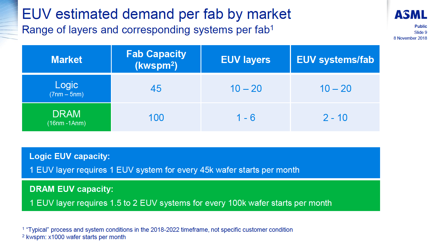
according to WikiChip, the plan is to use EUV for up to 12 layers for Intel 4. ASML reckons you need roughly 1 EUV system per layer for every ~45,000 wspm of fab capacity (these are older numbers but should encompass the NXE: 3400B/C scanner generations).
If yields were the problem, then Intel would just launch, but with lower volume. Intel's biggest issue right now is incompetence on the design side. It's why we get absurdities like Intel saying Intel 4 will be ready by end of '22 but we won't get products till H2'23.
I believe that the original POR for Meteor Lake was PRQ and HVM in H2'22 for an initial launch in Q1'23. Their statement during the Investor Meeting 2022 session was, "Meteor Lake CPU tile production stepping tape out" in H2'22. That's essentially not even committing to PRQ by the end of Q4'22, but it also does not rule out a Q2'23 launch, which is what many folks here were expecting anyway.
Looks like they changed the Meteorlake graphics architecture from DG2 based to Battlemage DG3 based. Good thing because the architecture in DG2 isn't particularly competitive.
Some say Raja will have a hard time since he was handed the "worst" GPU architecture in the industry.
I think many folks, Ryan included, are completely misreading those slides. The architecture in the IGPs is not the same as in the dGPUs that happen to be shipping during the same timeframe. They are separate products with concurrent shipping windows. Meteor Lake (and future IGP generations) will apparently be included under the Arc brand, but MTL is Xe LPG and ARL is Xe LPG Plus, which look to be Gen12.7, or the same Xe generation as DG2/Alchemist. Battlemage is Xe2 and looks to be based on Gen12.9 ELG. Celestial should be Xe3 based on Gen13 DG3, although I'm a little confused as to the future of DG2>DG3 and ATS>JPS with the insertion of ELG and the seeming resurrection of the Arctic Sound codename.
... Where did you see that the base die is using 10nm?
I'm not necessarily convinced. The only thing that even hints at such a change is both Meteor Lake and Battlemage showing up in the same column on a diagram with time/generation as the axis. I'd still bet that it uses DG2 IP.
Intel has stated on numerous occasions at this point that MTL is using second generation Foveros with a 36 µm bump pitch, a.k.a. Intel 7 FOVEROS / 1274.FV, or in other words "10nm". Are you expecting 22nm with a 36 µm bump pitch instead?
Also, I know you believe that the base die will act as a passive interposer, but then the PCH would have to be integrated into the SOC tile for at least the mobile parts. And that smaller tile above the CPU tile, which you claim serves an I/O purpose, is only 9.0 mm x 1.9 mm = 17.1 mm². That's in the ballpark of Thunderbolt 4 redriver chips that are designed to be embedded into cable connectors. I/O and analog tends to demonstrate worse area scaling than logic or SRAM, so what node do you think that little tile is on? In what universe would it not have been more cost effective to integrate that block into one of the other tiles? I guess with Foveros you're routing signals to the base tile using TSVs as opposed to needing to stick to the perimeter for wire-bonding, but still...
Yes, the Meteor Lake ones are different, which is why I spoke of Arrow Lake. These clearly are not Meteor Lake. Are you certain about 384 EUs for Arrow Lake? From what I've seen, most rumors were 320 EUs for Arrow Lake:
Intel Arrow Lake for mobile with powerful GPU AdoredTV claims to have the first information on mobile series succeeding Meteor Lake. Last week a list of supposed Intel product codenames has been making rounds on the tech news websites. The message that was originally shared on Reddit has since...

videocardz.com
but 384 EUs for the discrete GPU card:
Intel released driver for four unreleased integrated graphics cards, as well as the successor for the DG2 GPU family, "Elasti."

wccftech.com
Rumors pointed to 320 EUs, but the
GPU drivers seem to show the following configurations:
gen12-hp / xe_lpg
- MTL_1x4x16
- MTL_2x4x16
- MTL_3x4x16
gen12-hp / xe_lpgplus
- ARL_6x4x16
Which would be 384 EUs total, although Intel might decline to ship a fully enabled version.