Question [AT] AMD extends GloFo WSA to 2025

Page 5 - Seeking answers? Join the AnandTech community: where nearly half-a-million members share solutions and discuss the latest tech.

NostaSeronx

Diamond Member
Sep 18, 2011
3,683
1,218
136
If it was cheap, yeah. That's the problem. N7 doesn't look like it's going to be cheap any time soon.
N6 with increased EUV throughput is basically smashing towards sub-10nm.

Actual real world Mendocino is cheaper than a hypothetical Monet.

However, this is not the case with 22FDX/12FDX.
22FDX is a 30% price reduction compared to TSMC 28HP and GloFo 28SHP
12FDX is a 40% price reduction compared to GloFo/Samsung 14LPP, etc.

Since $10B Mubadala purchase of FinFET from Samsung:
2014: $1.5B loss
2015: $1.3B loss
2016: $0.4B loss
2017: $1.2B loss <-- AMD ramp
2018: $2.7B loss <-- GloFo peaks 14LPP production
2019: $1.3B loss <-- AMD shifts orders to TSMC(CPU/GPU)
2020: $1.3B loss <-- GloFo ramps up older nodes and more AMD to TSMC(APU/Semi-custom)
2021: $0.25B loss <-- GloFo provides boosted supply of older nodes
8 year average of ~1.3B loss

Meanwhile TSMC:
2014: $8.0B gain
2015: $9.7B gain
2016: $10.2B gain
2017: $11.6B gain
2018: $11.9B gain
2019: $11.8B gain
2020: $18.1B gain
2021: $21.0B gain

GloFo:
Increase what AMD pays via 12LP+/12LP++ super-price-hike.
Decrease what themselves pay via 12FDX lower-price but higher-profit.

TSMC:
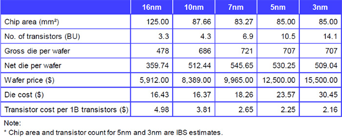
N7 is $9000
N6 is $6000
EUV machines go bbrrrrrrrrrrrttt:
tsmc7nm.jpg

14LPP/12LP/12LP+ has no high volume customers to go against the sub-50% utilization rate at Malta. Nor did FinFETs have any incentive caused by customer demand to go to China(failed Chengdu), Europe(Dresden), or Singapore(Woodlands)...
(Chengdu dropped because of Simgui and Zingsemi 300mm FDSOI wafers wouldn't be ready at 2019, basically both were targeting 2022-2023.
Simgui = 800K wafers
Zingsemi = 600K wafers

Soitec by Mid-2025:
Pasir Ris = +1M wafers
Bernin II = +1M wafers
3rd fab before FY26 = +1M wafers
All three fabs = ~7M FDSOI or RFSOI do to Leti/SOITEC FD on RF and RF on FD process)

12FDX has Automotive/Aerospace/Quantum-AI-NewCompute/Home/etc customers and more from 22FDX->12FDX track and 14LPP/12LP/12LP+->12FDX track.
$500M for a single year is a lot of wafers assuming 12LP+ is cheap (compared to TSMC). You figure demand for the existing Zen 3 products will be gone by 2025. Chromebooks would make sense but you figure Dali and Picasso won't cut it then. So that's where the discrepancy is.
As far as I can tell most demand for AMD is the quad-core Chromebooks (Picasso-C, etc). Dali/Pollock basically dropped dead. Which is probably why Picasso-H appeared in Tesla, because increased Chromebook led to more Picasso out.

3250C ~70$ to 3500C ~100$ given U-space => Same machine cost

The existence of Mendocino and Cezanne chromebooks and Raphael and Genoa moving away from GloFo IODs. Will cause GlobalFoundries a wafer throughput crash by -90% within 2023.
 
Last edited:

RTX

Member
Nov 5, 2020
90
40
61
Are these WSAs being used to continue supplying existing AMD products or entirely new ones?

Some of these have been discontinued.
All 10th gen are still being manufactured.
 

NostaSeronx

Diamond Member
Sep 18, 2011
3,683
1,218
136
Are these WSAs being used to continue supplying existing AMD products or entirely new ones?
WSA applies to existing and new ones.

Of the existing ones: 14nm/12nm (GF might end of supply this)
Of the new ones: Unknown (Only can be fabbed at GF)
Of the end of supply ones: 32nm/28nm (June 2020: End of Supply announced, July 2021: End of Supply began)
 

NostaSeronx

Diamond Member
Sep 18, 2011
3,683
1,218
136
Where did you get these wafer prices? Could you please share the link?
It is a mixture of CPR(Counterpoint Research), IBS(INTERNATIONAL BUSINESS STRATEGIES), and CSET(The Center for Security and Emerging Technologies).
12-inch-Wafer-Prices-by-Nodes-in-Leading-Foundries-2020-2022-1024x552.png

On the generalization of costs if 5nm isn't the cost of 10nm, then it is 6nm which is 7nm converted to EUV that is the cost of 10nm:
7nmDUV5nmEUV.png

Take note of FEOL and M4-M12 being the same: while MOL and M1-M3 drops in price:
7nmduvtoeuv.png
(imec expects 7nm DUV to be ~7000 and 7nm EUV to be ~5000 instead)

9000*~(4/5) => 7200 *~(97/100) => 6984, etc

Hence, the generalization of 7nm = ~9000 and 6nm = ~6000. This is added by 125 wph tools getting Tput upgrades up to ~225 wph, thus reducing the costs more.
 
Last edited:
  • Like
Reactions: Hougy and maddie

NostaSeronx

Diamond Member
Sep 18, 2011
3,683
1,218
136
Um... i'd expect N6 to cost more than N7, not less. Possibly not a lot more but more.
N6 had a early point of costing more than N7, but as time goes on N6 should get cheaper faster than N7. We have already flown past the cost crossover in 2020, so...

N7 has static wph since iArF tools are at their limit.
N6 has growing wph since EUV tools aren't at their limit.

Less masks, less process steps, less lead time => More production. 1xN7 ~9000$ wafer is replaced by ~3xN6 ~6000$ wafers in the same time.

28nm ~10000$ in 2011 to 28nm ~<3000$ in 2021
7nm DUV ~10000$ in 2018 to ~9000$ in 2028.
7nm EUV ~8000$ in 2020 to ~<4000$ in 2028.
Is the general expectation, as EUV allows for 7nm to replace 28nm as costs drop for EUV but not for iArF.

150K WPM[3 modules] for N7 (then) to 500K WPM N6[9 modules] (later) generally on a HVM increase at that scale causes a price reduction.
 
Last edited:
  • Like
Reactions: maddie

Doug S

Platinum Member
Feb 8, 2020
2,203
3,405
136
Which means more wafer output, not lower prices. As the graphs show TSMC is charging MORE in 2022 than in 2021 for N7 wafers.

Having fewer process steps also means it costs them less per wafer to make. Whether that translates into lower prices for their customers is a separate question. TSMC wants to encourage people to move off N7 because it costs them more to make, and they can make more of it. For that reason they consider N6 the long term version of the N7 family. So they have reason to make N7 cost more than N6 even beyond the difference in their production cost.

If a business has more more demand than it can serve there are three choices: 1) raise prices to reduce the demand to match what it can supply; 2) let a line form out the door and going down the block; 3) increase supply to match the increased demand (and hope that increased demand isn't temporary) That last is not really an option for TSMC in the short term, since new fab capacity takes a while to come online and fab machinery also has more demand than there is supply. So they've chosen option 1 for now, and can use the extra money they get to not only line their pockets but also accelerate making option 3 a reality.
 
  • Like
Reactions: Saylick and Tlh97

Mopetar

Diamond Member
Jan 31, 2011
7,797
5,899
136
Wasn't TSMC planning to convert their N7 to N6 as time moves on? Regardless of price, everyone is screaming for more wafers and increasing the throughput is the best way to accomplish that in the short term. TSMC could use pricing to nudge customers in that direction. Otherwise lines that keep making N7 are taking up valuable fab space that could be used for N6.
 

moinmoin

Diamond Member
Jun 1, 2017
4,934
7,619
136
Wasn't TSMC planning to convert their N7 to N6 as time moves on?
Don't think so, you can't exactly convert DUV equipment to EUV. And TSMC usually keeps existing capacity for quite some time, not converting them to other nodes. But TSMC itself called N7 to be targeting the high performance market and N6 to be targeting the mainstream market. And due to fewer layers it's easier (and very likely also cheaper) for TSMC to expand the throughput for N6 than N7.
 

Doug S

Platinum Member
Feb 8, 2020
2,203
3,405
136
Wasn't TSMC planning to convert their N7 to N6 as time moves on? Regardless of price, everyone is screaming for more wafers and increasing the throughput is the best way to accomplish that in the short term. TSMC could use pricing to nudge customers in that direction. Otherwise lines that keep making N7 are taking up valuable fab space that could be used for N6.

They do that by encouraging customers to make the choice to move. But they can't force e.g. Apple to move their older N7 stuff like the A12X used in the latest Apple TV to N6. I wouldn't be surprised if they retire the N7 process entirely in favor of N6 someday, but they would have to give customers years of notice.
 

Mopetar

Diamond Member
Jan 31, 2011
7,797
5,899
136
Don't think so, you can't exactly convert DUV equipment to EUV. And TSMC usually keeps existing capacity for quite some time, not converting them to other nodes. But TSMC itself called N7 to be targeting the high performance market and N6 to be targeting the mainstream market. And due to fewer layers it's easier (and very likely also cheaper) for TSMC to expand the throughput for N6 than N7.

Some of the equipment can be reused, so they'd sell whatever they won't use as they purchase more EUV equipment.

The reason to phase out 7nm is that they can use the facilities originally build for 7nm to house 6nm. Building new fabs to expand 6nm capacity while leaving 7nm in place is too costly and would take too long to complete.

They do that by encouraging customers to make the choice to move. But they can't force e.g. Apple to move their older N7 stuff like the A12X used in the latest Apple TV to N6. I wouldn't be surprised if they retire the N7 process entirely in favor of N6 someday, but they would have to give customers years of notice.

They can use prices to incentivize behavior. If making a new set of masks and updating to 6nm saves the companies who buy the wafers some money, they'll make that move instead of just sticking with 7nm.

If the throughput is significantly better, TSMC can make more even selling those wafers at a lower cost.
 
  • Like
Reactions: Tlh97

NostaSeronx

Diamond Member
Sep 18, 2011
3,683
1,218
136
Got in good word, that it is finally happening.

"GlobalFoundries is seeking to fill the role of SMTS Lithography Process Engineer to drive technology readiness for 22FDX in Fab8 to support 5G applications in mobile devices. This experienced process engineering role will be primarily responsible for leading both development of 22FDX towards technology milestones and rapid qualification across new tools during planned fab expansion." - A week ago(24/03/2022 14:05:07)
There is an extentsion but it is part of the Fotonix (Photonics) part of the listing.

22FDX is appearing at Fab8 soon-ish.

From what I have got/heard is that 22FDX/12FDX at Fab8 will be announced together.
- 22FDX will get half of 14LPP/12LP/12LP+ to itself.
- 12FDX will share the remaining wafers with 14LPP/12LP/12LP+.

Fotonix, 22FDX, and 12FDX are expected to accrue enough wins to afford Fab 8 Module 2. Which will be used to expand Fotonix/22FDX/12FDX and do "NextFDX".

With an aggressive FDXcelerator 2.0 program to get everyone off FinFETs as quickly as possible. There is no roadmap beyond 12LP+ for FinFETs and funding value-adding features for it is supposedly ending to support 12FDX instead.

Primary nodes:
12LP+ (FinFET), 12FDX (FDSOI), 45FTX (PDSOI), 45SG (SiGe HBT)

Secondary nodes:
14LPP/12LP (FinFET), 22FDX (FDSOI), 45FTX2 (FDSOI), 90RH (FDSOI)

Bolded are the nodes that will survive the hard pivot(abandoning existing HVM(14nm/12nm FinFET), rather than non-existing HVM(7LP and beyond)) at GlobalFoundries Malta. There are other nodes that are on the Tertiary side but basically I'm pretty sure you can guess the wafer type.

Minimum of a migration tapeout(12LP+ to 12FDX) based off old numbers:
* Same area
* +7% average performance
* -10% average power
* -25% per die cost
 
Last edited:

moinmoin

Diamond Member
Jun 1, 2017
4,934
7,619
136
The reason to phase out 7nm is that they can use the facilities originally build for 7nm to house 6nm. Building new fabs to expand 6nm capacity while leaving 7nm in place is too costly and would take too long to complete.
Again, that's not how TSMC is operating. TSMC is not using Intel's (now with IFS 2.0 past?) way of constantly ramping up and then rather quickly converting different nodes. TSMC is ramping up new nodes and then keeping the capacity for years to come. N7 is still a highly requested node that rather demands for further capacity expansion, not phasing out and conversions (which TSMC isn't doing anyway).
 
  • Like
Reactions: Tlh97 and scineram

NTMBK

Lifer
Nov 14, 2011
10,208
4,940
136
Could a new PS5 launch soon or is the cost of creating a the new masks not worth it? What would it use? N5? N6?

I doubt we'll see if before 3nm class processes, but I could be wrong. They certainly won't use anything that GlobalFloundering can manufacture, so this is probably the wrong thread to discuss it ;)
 

NostaSeronx

Diamond Member
Sep 18, 2011
3,683
1,218
136

Mopetar

Diamond Member
Jan 31, 2011
7,797
5,899
136
Again, that's not how TSMC is operating. TSMC is not using Intel's (now with IFS 2.0 past?) way of constantly ramping up and then rather quickly converting different nodes. TSMC is ramping up new nodes and then keeping the capacity for years to come. N7 is still a highly requested node that rather demands for further capacity expansion, not phasing out and conversions (which TSMC isn't doing anyway).

If it's highly requested isn't there an even greater reason to transition as much of it as possible to N6 for greater throughput? It has the same design rules as N7, the only thing you would need are new masks. If you aren't using N7 right now there's not a lot of reason to jump on board since N6 would require fewer mask layers (saves money) outside of price differences. But from TSMC's perspective they want to sell as many wafers as possible and if N6 lets them do that, they have a reason to push customers in that direction.
 
  • Like
Reactions: Tlh97

NostaSeronx

Diamond Member
Sep 18, 2011
3,683
1,218
136
An update with new nodes supposedly scheduled for end of the year.

Old nodes, Malta-only:
14LPe/14LPP/12LP/12LP+

New nodes to be announced, Dresden+Malta:
11LP/11LPM/12FDX

The safest assumption is 11LP/11LPM is Bulk FinFET... however, the switch from Leading Performance to Low Power might imply a full return to planar.

Example purposes:
12FDX => SHP class-node, Planar+SOI+High Mobility
11LPM => HPP class-node, Planar+Bulk+High Mobility+DDC/SSRW
11LP => SLP class-node, Planar+Bulk+DDC/SSRW
Basically all of them being 10-nm Planar Gate + 56nm minimum metal pitch

As well as potential everything being planar GAA-related:
2-Figure1-1.png

The switch to planar impacts 3D Logic scaling, as planar-type nodes do not thermally couple as hard between logic dies.

For example rather than a Planar Monet, it is more likely to see a 3D Monet.
Top-die (high heat logic/CPU die) => Quad-core Zen('number') die
Middle-die (low heat GPU/Multimedia/Vision die) => A couple WGPs
Bottom-die (low-heat I/O die) => everything else needed.
Three small dies has nearer to linear costs rather than one gigantic planar die, etc.

However, I believe based on a couple mentions regarding LP cores from AMD on linkedin and a couple references of GloFo 12FDX at Malta:
12fdxatmalta.png

That the 3D CCD will not be Zen but more likely derivative of Fam 16h with actual CMT2:
Shared Front-end, Split Decode, Shared Retire/Rename, Split Scheduler/Execution for Int-clusters and FP-clusters, Shared Load-Store/Bus/L2.

Same performance class as Zen, but more aggressive area/power optimization:
14nm Jaguar = 1.8 mm2
14nm Zen = 5.5 mm2
12FDX Ultra-low-power CMT2 = Less than or equal to half of 14nm Zen.
Two core/quad-cluster = ~5 mm2 and 2 MB L2 = ~ 6 mm2 = ~11 mm2 + ~11 mm2 + ~16 mm2 or smaller for 8 MB L3 => ~38 mm2.

The range for dies I got via estimation were 48 mm2 to 64 mm2, but all dies should be similar with bottom IOD being biggest, GCD mid, and CCD being smallest.

CCD+CCD+IOD = Server-orientated
CCD+GCD+IOD = Consumer-orientated
GCD+GCD+IOD = Graphics-orientated

150 mm2 / $4000 (14nm/12nm FF) = 386 good dies which is greater than $12.01.
64 mm2 / $3000 (12FDX/11nm planar) = 860 good dies which needs three costs given are then greater than $10.47.

From Dual-core Zen+3 CU GCN to Quad-core Zen('number')/4 CU RDNA('number') while reducing price. With a more aggressive stance in shrinking area/power. ~51.2 mm2 / $3000 = 1096 good dies which needs three and given costs would be $8.21 which is a 0.68x drop in price just for the die.

Which means going More than Moore/3D-stacking is the clear solution if GloFo wants AMD still. It also allows AMD to reduce costs while given a more expensive node than 28nm/22nm.
strategywsa.jpg

NGFXShowcase:
fx2.jpeg

CPU die = ~60 mm2
IOD die = ~60 mm2
CPU clock = ~4.7 GHz
CPU power = ~35W

Edit: I have a further list of approved nodes that will be launching second half 2022:

22FDX+; New Track Height (potentially, 6T or 7T)
22FDX++; Reduced CPP, same BEOL, re-uses 12FDX's new gate/SOI materials
12LP++; New Track Height (same as 22FDX+), more aggressive SDB/CNRX in standard cells.
11LP/11LPM: Low-power, Low-power+Mobility-enhancements;
Same as 12FDX but uses a local poly-crystalline layer instead of wafer length oxide under the gate(Deeply Depleted Channel/SSRW channel/etc)
The bulk hybrid layer of 12FDX should be able to 11LP transistors:
Bulk planar transistors => Low static leakage, high dynamic leakage
SOI planar transistors => High static leakage, low dynamic leakage
 
Last edited: