AMD “Next Horizon Event" Thread

Page 2 - Seeking answers? Join the AnandTech community: where nearly half-a-million members share solutions and discuss the latest tech.

Topweasel

Diamond Member
Oct 19, 2000
5,436
1,654
136
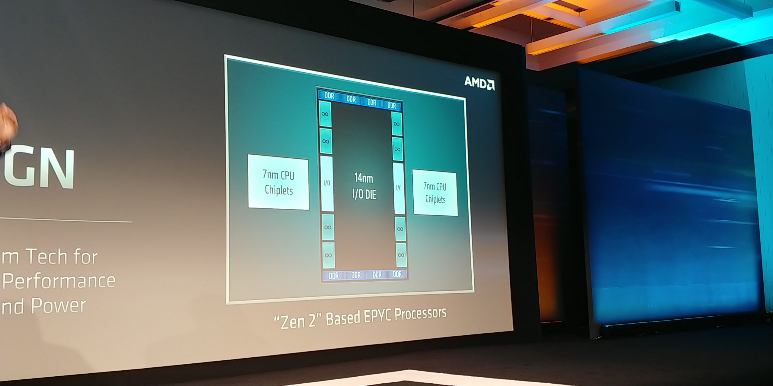
The next big question I have is how much cache does that IO die have? To host all that IO, it needs a large circumference. So a lot would fit, even at 14nm.

Hell it could 1x or 2x Zen 1 die size and it still might be a major space saver. A Normal Zen die is 190mm. Just the space saving (2x) you have it at 95mm. Take out all that IO stuff maybe you can get it down to 65mm.
 

Despoiler

Golden Member
Nov 10, 2007
1,966
770
136
Did I hear him say MI60 can do workloads down to 1bit precision?

ROCm 2.0 and it's upstreamed. That is huge!
 
  • Like
Reactions: lightmanek

Despoiler

Golden Member
Nov 10, 2007
1,966
770
136
MI60

7.4 TFLOPS FP64
14.7 TFLOPS FP32
118 TOPS INT4

Shipping this quarter
 

BigDaveX

Senior member
Jun 12, 2014
440
216
116
Good numbers on MI60's theoretical compute power, but then Vega was already ahead of Pascal on that metric, and was generally slower in games. Got a feeling it's still gonna be a case of gamers going nVidia and miners going AMD.

Much more impressive on the CPU side; this is feeling a lot more like the company that spent most of the first half of the 2000s curb-stomping Intel.
 

Paratus

Lifer
Jun 4, 2004
16,613
13,295
146
MI60

7.4 TFLOPS FP64
14.7 TFLOPS FP32
118 TOPS INT4
Water cooled Vega 64 had 12.5B transistors and did 13.7TFLOPS @510mm2

So 5.6% more transistors and 7.3% more theoretical performance with 35% smaller die.

Not bad.
 

lixlax

Member
Nov 6, 2014
183
150
116
Water cooled Vega 64 had 12.5B transistors and did 13.7TFLOPS @510mm2

So 5.6% more transistors and 7.3% more theoretical performance with 35% smaller die.

Not bad.
Doesn't look impressive at first, but it probably consumes less than 50% of power compared to Vega 64 LC.
 
  • Like
Reactions: lightmanek

Asterox

Golden Member
May 15, 2012
1,026
1,775
136
A wide(r) core, finally :)

And as i see, the most important Zen 2/8 Core per CCX for AM4 socket is now confirmed.

"Faster, Smaller, Lower Power Transistors (2x Density, 0.5x Power, 1.25x Performance at same performance/power)
Multiple Products in Development
Deep Partnership with TSMC and Design Automation Vendors
AMD has made significant changes to their CPU architecture which help deliver twice the throughput of their first generation Zen architecture. The major points include an entirely redesigned execution pipeline, major floating point advances with doubled the floating point to 256-bit and double bandwidth for load/store units. One of the key upgrades for Zen 2 is the doubling of the core density which means we are now looking at 2x the core count for each core complex (CCX) which will now be risen to 8 per CCX compared to 4 per CCX.

Improved Execution Pipeline
Doubled Floating Point (256-bit) and Load/Store (Doubled Bandwidth)
Doubled Core Density
Half the Energy Per Operation
Improved Branch Prediction
Better Instruction Pre-Fetching
Re-Optimized Instruction Cache
Larger Op Cache
Increased Dispatch / Retire Bandwidth
Maintaining High Throughput for All Modes"
 

ub4ty

Senior member
Jun 21, 2017
749
898
96
K, so obvious question is obvious....
Infinity fabric link CPU<->GPU...

How exactly are they going to physically pull this off? Mobo level? cable? What of the generic PCIE interface? Augmented? Some type of nearby connection? Something over PCIE 4.0?

What is the physical connection going to look like here?

For reference, what I'm looking to see from AMD (Nvidia's NVlink tech) :
mmi20170200402.gif


6965821-15114088622690742_origin.png


Have they detailed this yet? Is this going to flow down to consumer zen2 or be cut out and delayed? Seems all the mobos would have incompatibility as this is board level?
 
Mar 11, 2004
23,030
5,495
146
Good numbers on MI60's theoretical compute power, but then Vega was already ahead of Pascal on that metric, and was generally slower in games. Got a feeling it's still gonna be a case of gamers going nVidia and miners going AMD.

Much more impressive on the CPU side; this is feeling a lot more like the company that spent most of the first half of the 2000s curb-stomping Intel.

Vega 20 is not a gamer card so no need to even speculate that people might buy more Nvidia cards for gaming than Vega 20s. Navi is mainstream class, and hopefully should offer at least GTX1080 performance for say $300. If it can push above that they could even probably sell it in the $300-400 range until Nvidia gets 7nm GPUs out (or if Nvidia cuts prices on RTX, putting the 2070 ~$400). AMD won't have a new large gamer GPU til likely 2020 with Navi (forget if its 10 or 20 that's supposed to be the larger one). There was some talk about mGPU, but not sure that will help gaming.
 

ub4ty

Senior member
Jun 21, 2017
749
898
96
Vega 20 is not a gamer card so no need to even speculate that people might buy more Nvidia cards for gaming than Vega 20s. Navi is mainstream class, and hopefully should offer at least GTX1080 performance for say $300. If it can push above that they could even probably sell it in the $300-400 range until Nvidia gets 7nm GPUs out (or if Nvidia cuts prices on RTX, putting the 2070 ~$400). AMD won't have a new large gamer GPU til likely 2020 with Navi (forget if its 10 or 20 that's supposed to be the larger one). There was some talk about mGPU, but not sure that will help gaming.

Seems they're leaving a lot on the table if that's the case given that Zen2 is PCIE 4.0 and all of the other goodies : infinity fabric CPU/GPU? Is this a point in which AMD will start to focus moreso on profits and segmentation where the pro CPUs/GPUs start to have clear features distinguished from consumer line? What's this event spell for consumer line? We have 8 cores per CCX now... Will consumer side see a doubling too or just a shrink? Any potential for exotic add-ons to the chiplet like HBM? GPU complex? What will AMD do w/ all of the newly available space on consumer Zen2? What does consumer Zen2 look like?
 

Saylick

Diamond Member
Sep 10, 2012
3,084
6,184
136
And as i see, the most important Zen 2/8 Core per CCX for AM4 socket is now confirmed.

"Faster, Smaller, Lower Power Transistors (2x Density, 0.5x Power, 1.25x Performance at same performance/power)
Multiple Products in Development
Deep Partnership with TSMC and Design Automation Vendors
AMD has made significant changes to their CPU architecture which help deliver twice the throughput of their first generation Zen architecture. The major points include an entirely redesigned execution pipeline, major floating point advances with doubled the floating point to 256-bit and double bandwidth for load/store units. One of the key upgrades for Zen 2 is the doubling of the core density which means we are now looking at 2x the core count for each core complex (CCX) which will now be risen to 8 per CCX compared to 4 per CCX.

Improved Execution Pipeline
Doubled Floating Point (256-bit) and Load/Store (Doubled Bandwidth)
Doubled Core Density
Half the Energy Per Operation
Improved Branch Prediction
Better Instruction Pre-Fetching
Re-Optimized Instruction Cache
Larger Op Cache
Increased Dispatch / Retire Bandwidth
Maintaining High Throughput for All Modes"

I'm still not sure how WCCFTech came up with 8-core CCX from "doubled core density". It could just mean 8 chiplets x 8 cores/chiplet for 64C for EPYC 2, OR it could mean 4 chiplets x 16 cores/chiplet... The number of cores/CCX is still not confirmed. Core density can be measured at the CCX level, at the chiplet level, or even at the package level.
 

tamz_msc

Diamond Member
Jan 5, 2017
3,708
3,554
136
K, so obvious question is obvious....
Infinity fabric link CPU<->GPU...

How exactly are they going to physically pull this off? Mobo level? cable? What of the generic PCIE interface? Augmented? Some type of nearby connection? Something over PCIE 4.0?

What is the physical connection going to look like here?

For reference, what I'm looking to see from AMD (Nvidia's NVlink tech) :
mmi20170200402.gif


6965821-15114088622690742_origin.png


Have they detailed this yet? Is this going to flow down to consumer zen2 or be cut out and delayed? Seems all the mobos would have incompatibility as this is board level?
It would seem that the IF-GPU link is similar in principle to NV-link, though details regarding NV-link is scarce.
 

tamz_msc

Diamond Member
Jan 5, 2017
3,708
3,554
136
I'm still not sure how WCCFTech came up with 8-core CCX from "doubled core density". It could just mean 8 chiplets x 8 cores/chiplet for 64C for EPYC 2, OR it could mean 4 chiplets x 16 cores/chiplet... The number of cores/CCX is still not confirmed. Core density can be measured at the CCX level, at the chiplet level, or even at the package level.
This picture likely points to 8 8-core chiplets due to the eight IF links surrounding the I/O die.

20181106_174654_HDR.jpg
 

NostaSeronx

Diamond Member
Sep 18, 2011
3,683
1,218
136
Infinity Fabric operates through virtual-physical linkage of Infinity Fabric InterSocket.

PCIE 4.0 or IF or both, etc.
 
  • Like
Reactions: ub4ty

HurleyBird

Platinum Member
Apr 22, 2003
2,670
1,250
136
Yeah, 8 core CCX seems like an assumption. My guess is that whatever is inside each chiplet doesn't look like the traditional CCX layout and that the L3 is unified between all eight cores, since that seems like obvious low hanging fruit, but there are a number of topologies that could enable that.
 

Saylick

Diamond Member
Sep 10, 2012
3,084
6,184
136
This picture likely points to 8 8-core chiplets due to the eight IF links surrounding the I/O die.
/snip
8x8 makes perfect sense to me because:
1) 4C CCX keeps things simple with respect to the number of interconnects between cores, and reduces the development cost from Zen 1
2) 2-CCX or 8C desktop parts will still be the norm for most consumers. If AMD went with a 8C CCX approach, it'd be overkill for consumers.
3) Threadripper can still use a MCM approach with up to 32 cores (4 dies w/ 8 cores each).

Basically, only EPYC 2 would use a chiplet approach. All other Zen 2 products remain similar to Zen 1 but with improved IF, IPC, clocks, power efficiency, etc.
 
  • Like
Reactions: Lodix

ub4ty

Senior member
Jun 21, 2017
749
898
96
Infinity Fabric operates through virtual-physical linkage of Infinity Fabric InterSocket.

PCIE 4.0 or IF or both, etc.
So, the mode is switchable in hardware?
Issue is... PCIE 4.0 is still a physical interface.
So, IF local on CPU complex over Phy is not the same as the external variant that would have to probably be encap'd over PCIE 4.0...

My main inquiry is about the physical interface when Infinity fabric is exposed off chip.
 

Asterox

Golden Member
May 15, 2012
1,026
1,775
136
I'm still not sure how WCCFTech came up with 8-core CCX from "doubled core density". It could just mean 8 chiplets x 8 cores/chiplet for 64C for EPYC 2, OR it could mean 4 chiplets x 16 cores/chiplet... The number of cores/CCX is still not confirmed. Core density can be measured at the CCX level, at the chiplet level, or even at the package level.

Threadriper 2990WX has four CCX or each CCX has 8 Cores, as also Rome/Epyc 2 same thing 8 Core CCX as we see.

WCCFTech is not that drunk, "they must now this facts" so what is missing or only Desktop Ryzen 2/Zen 2.