Question Zen 6 Speculation Thread

Page 363 - Seeking answers? Join the AnandTech community: where nearly half-a-million members share solutions and discuss the latest tech.

Covfefe

Member
Jul 23, 2025
123
220
76
It really depends on the speed of the LPDDR5X modules. 8.5...9.6 Gbps are getting standard. 12.7 Gps is the ceiling. Strix Point mostly uses 7.5 Gbps modules and many notebooks also slow 5.6 Gbps modules.
  • 8.5...9.6 Gbps = 1.14...1.28x bandwidth vs. 7.5 Gbps
  • 10.7...12.7 Gbps = 1.43...1.69x bandwidth
The bigger L1 and L2 caches should be very effective. Compared to Strix Point without MALL it will be a very decent upgrade in bandwidth efficiency.
If then the universal compression comes into play, there should be another bandwidth amplification.

We do not know overall bandwidth efficiency upgrades. But summing all up together it could be on par with RDNA3 + 32 MByte MALL or at least close to it. AT4 could reach N44 performance levels.
  • RX 9060 XT has 320 GB/s memory bandwith
  • RX 9060 has 288 GB/s memory bandwith
  • 128bit LPDDR5X with 8.5 Gbps yields in 171 GB/s
  • 128bit LPDDR5X with 9.6 Gbps yields in 192 GB/s
  • 128bit LPDDR5X with 10.7 Gbps yields in 214 GB/s
  • 128bit LPDDR5X with 12.7 Gbps yields in 254 GB/s
  • 192bit LPDDR6 with 10.67 Gbps yields in 284 GB/s (effective) --> probably enough bandwidth for a desktop grade part with high clock rates (AMD should have designed / dimensioned it that way)
  • 192bit LPDDR6 with 12.8 Gbps yields in 340 GB/s (effective)
9.6 Gbps bandwidth for a mobile part might be a little bit tight. That is true. But as I said, we simply do not know RDNA5's overall bandwidth efficiency. Maybe LPDDR6 bandwidth levels are plenty enough and LPDDR5X is then sufficient for mobile parts with restricted TDPs. If 12.7 Gbps LPDDR5X gets used (but this memory is probably too expensive and not used), there should be no big difference in bandwidth compared to 10.67 Gbps LPDDR6.
Maybe I'm missing something, but your LPDDR bandwidth figures all look off.
  • LPDDR5X-9600 is 9.6*128/8 = 153GB/s.
  • LPDDR5X-12700 is 12.7*128/8 = 203GB/s.
  • LPDDR6-10667 is 10.667*192/8 = 256GB/s line speed, or 256 *256/288 = 228GB/s effective bandwidth.
 

basix

Senior member
Oct 4, 2024
342
671
96
You are right, I somehow assumed 128 GB/s at 6.4 Gbps instead of 102.4 GB/s.

I fixed it in the original post.

But the general idea is still valid:
If LPDDR6 with 10.67 Gbps works out for a desktop grade product, LPDDR5X should be OK enough for a mobile part in most cases.
 
Last edited:

ToTTenTranz

Senior member
Feb 4, 2021
963
1,583
136
L5X is gonna be around for a very long time, will steadily trickle down the pricing ladder but high volume stuff won't switch to LP6 until 2030+

Why? We're already getting LPDDR6 this year with the Snapdragon 8 Elite Gen 6 Pro / SM8975 and probably Mediatek 9600.

LPDDR5X took less than a year between being in the first smartphone and going into most higher-end laptop chips (Raptor Lake H/U and Phoenix).
Why would the PC market quadruple the latency to adopt the new memory standard, this time?
 

adroc_thurston

Diamond Member
Jul 2, 2023
8,670
11,373
106
Isn't 48bit LPDDR6 going to be at least as fast, if not faster than 64bit LPDDR5X at a lower power?
No, LP6 barely pushes pin rates up.
This ought to be a reason to accelerate adoption rate for mid/high end smartphones, not slow it down.
No, LP6 is not coming to mainstream SoCs for a long long while due to catastrophic PHY area efficiency.
 

basix

Senior member
Oct 4, 2024
342
671
96
No, LP6 is not coming to mainstream SoCs for a long long while due to catastrophic PHY area efficiency.
Why are LP6 PHY area inefficient? Compared to LP5X I do not see any obvious reason.

If you want to say that area efficiency is on par with LPDDR5X (bandwidth per area) or not much better, OK.
 
Last edited:

Doug S

Diamond Member
Feb 8, 2020
3,856
6,810
136
Forgot to source it. You can find it clearly from Synopsys data sheet for the combo PHY here: https://www.synopsys.com/dw/doc.php/ds/c/dwc_lpddr6_5_5x_5_phy_ds.pdf Bottom of page 2.

You have to give them your phone number and email for the download, but they don't actually check anything except that they are potentially valid, you can just use throwaways if you want to.

OK so that's how I originally thought they worked, then someone here told me I was wrong about that - plus I later saw some article claiming the same. So I assumed they'd figured out some way to do something like a 96 bit wide combo controller that provided either 6 LPDDR5X or 4 LPDDR6 channels.

If that's not the case then for the case of a combo controller then LPDDR6 is better because it makes more efficient use of that resource. If you design with an LPDDR6 only controller though then there's no benefit - because the chip area and shoreline used 96 bits worth of LPDDR6 controller and 96 bits worth of LPDDR5X controller are essentially the same. I know that's not relevant to AMD since they are probably going to be forced to do combo controllers to provide OEM flexibility but not everyone will be forced to go that way.
 

Tuna-Fish

Golden Member
Mar 4, 2011
1,697
2,617
136
If you design with an LPDDR6 only controller though then there's no benefit - because the chip area and shoreline used 96 bits worth of LPDDR6 controller and 96 bits worth of LPDDR5X controller are essentially the same.
They are not. The DQ pins are not the only pins on the interface. LPDDR5X has 72 active signals per 32-bit dual channel controller, while LPDDR6 has 84 active signals per 48-bit dual channel (4x half channel) interface. 3/2 data signals but only 7/6 times the pins. Or, 96-bit LPDDR6 uses only 168 signals, while 96-bit LPDDR5X uses 216. Even after you adjust for the 8/9 loss of efficiency from sharing the DQ pins, LPDDR6 comes out ahead.

LPDDR6 is a neat and efficient design.
 

MS_AT

Senior member
Jul 15, 2024
943
1,871
96
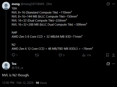
wishful thinking -> 48 + 3*48 = 192mb per CCD
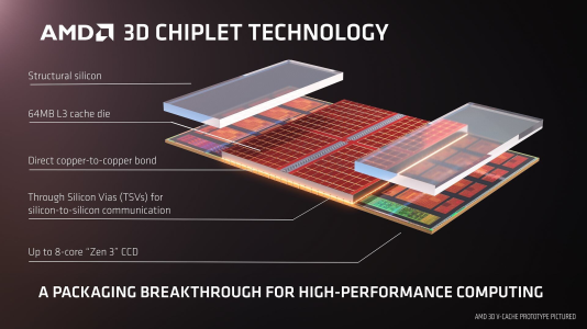
Wouldn't that be less technical feasible? I mean atm they are using 1L 64MB die. I guess stacking 2 of those, if they wanted to stack would have been easier than producing smaller 48MB dies and stacking those 3 times. If for some reason, they would need L3 areas to match, so 48MB in CCD and 48MB in X3D die, then to recoup the capacity I could envision them doing 2L, so 96MB of additional L3. That is 144MB of L3 in total, matching Intel in marketing wars, and easier to produce.
 
  • Like
Reactions: lightmanek

Joe NYC

Diamond Member
Jun 26, 2021
4,253
5,879
136
Some ppl also said no "such thing" to 9950X3D2 also if memory serves me right;)
But yea, only wishful thinking/hoping from me on this one.. But they could if they really wanted / was under pressure from bLLC size

That would certainly be a dream for AMD if they managed to sucker Intel into L3 size competition, where AMD would be stacking cheaper dies with low latency SRAM, while Intel is ballooning the N2 die size and increasing latency.
 
  • Haha
Reactions: lightmanek

Z O X

Member
Oct 31, 2022
40
48
61
One generation of the cache chiplet matching CCD size is not "always an exact match". Zen6 could move the cache back on top, or use structural silicon underneath.
Why not on both sides for cache galore?
It is always an exact match since they moved to wafer on wafer stacking.
So it's 48MB L3 in one plane and only 2*64MB underneath the whole CCD area (L3+12 cores)?
Doesn't seem logical or am I missing something...

Edit: correction
 
Last edited: