- Mar 3, 2017
- 1,779
- 6,798
- 136
I suspect Cinebench would be fine if there were only core-private caches.Cinebench would be doing just as fine
They surely ran lots of simulations, leaving uncertainty mostly to the question how well the investigated workloads overlap with customers' workloads.I happen to think the second option is more likely because AMD believes the cases with optimal resource allocation will outweigh the other ones.
That may sound weird, but Zen5 cluster interconnect is designed to be explicitly modular, goes from 4 to 16 cores.
?I also know that it ain't cheap to redesign anything in modern manufacturing processes.
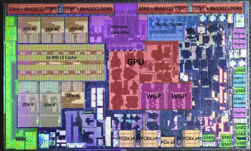
The ring isn't provisioned for scaling seamlessly like that.Look how AMD did reuse full 8-ring stop cpu ring for Phoenix2 instead of designing 6-stop reduced cache version for such a cost-oriented cpu - design costs seems to play big role.
Mmm, it’s starting to make sense to me about that ladder cache then. Basically introduce additional horizontal rungs so that portions of the ladder can be lopped off based on how many cores you want in the CCX.That may sound weird, but Zen5 cluster interconnect is designed to be explicitly modular, goes from 4 to 16 cores.


P-core boost differences are typically very small, especially if all of the cores are in close proximity on the same piece of silicon. That's just max boost though which doesn't come into play in this context because you're not hitting max boost clocks past 1 - 2 cores being loaded. Then the question becomes, what is the 3 - 4 cores boost frequency of the P-cores? If the C-cores can't hit that same frequency, it makes no sense to have a 2p4c+2p4c split because you'd have a significant drop-off in performance past 2 cores being loaded. If the C-cores can hit that frequency but are at the end of their frequency range and thus less efficient than the P-cores in that range, then it makes no sense to have a 2p4c+2p4c split because you are using more power for no performance improvement. Additionally, once you move to the 2nd CCX, you are now bringing in 2 P-cores that will never boost above a 7-8 core loaded frequency, which the C-cores could easily achieve, so why make them P-cores at all? You are then using more space for no performance or efficiency gain. The proposed configuration makes no sense.
On AMD the differences are actually quite large. more than 300 Mhz on my 7950X. Only 2 of my cores can hit the 5.75 ghz. The worst of the bunch can technically hit 5.5. ghz, but rarely ever comes close.
At least 1 of my cores hits 6ghz with a bit of prodding (read: overclocking magic, though I run stock)
In this case you're talking about 2 different pieces of silicon that I'm pretty sure AMD bins for 1 fast and 1 slow. Considering the difference is <5% even in this case, that's pretty close. The difference will be even tighter on the same silicon and much smaller than the jump down to a C-core speed.
Even on the same chiplet there are wide variations.
I wasn’t intending to compare it to Zen4C, I was merely stating that there is absolutely a significant difference between P-Cores.
What makes you think so? That'd essentially be margin of error level. If that were the case the whole effort of designating preferred cores etc. going on since the first Zen gen in CPPC and Ryzen Master would be a sure waste.On the same CCD I would expect the cores to have a spread of ~2% at most, though probably less than 1% (assuming adequate cooling). When dealing with a 7950x, that means around 100 - 125 MHz max boost difference but probably closer to 50 MHz.
What makes you think so? That'd essentially be margin of error level. If that were the case the whole effort of designating preferred cores etc. going on since the first Zen gen in CPPC and Ryzen Master would be a sure waste.
?
It's not that expensive.
The ring isn't provisioned for scaling seamlessly like that.

The. Ring. Is. Not. Provisioned. For. <8 stop. Operation.What do you mean?
They are used, ring only connects L3 slices, not cores.there's 8-slice L3 ring probably directly from bigger Phoenix. Ring still works fine even if some of ring client slots are unused.
The. Ring. Is. Not. Provisioned. For. <8 stop. Operation.
Got it?
They are used, ring only connects L3 slices, not cores.
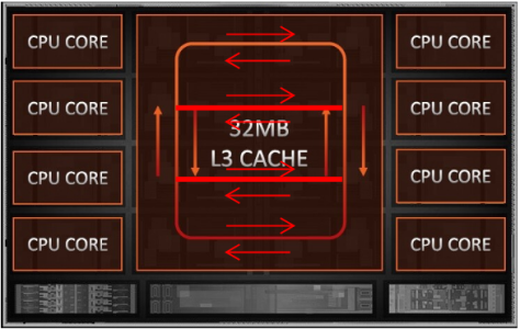
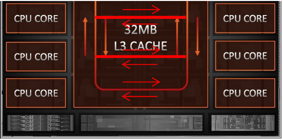
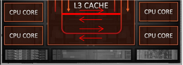
I've no idea if that is what AMD is doing but IBM surely did that for their racetrack ring in Power10 and (I think) Telum.Edit: Adding some images to explain.
8 cores:

6 cores:

4 cores:

Mmm, it’s starting to make sense to me about that ladder cache then. Basically introduce additional horizontal rungs so that portions of the ladder can be lopped off based on how many cores you want in the CCX.
Edit: Adding some images to explain.
8 cores:
View attachment 91691
6 cores:
View attachment 91692
4 cores:
View attachment 91693
Looks aimed at the OEM market. Which is interesting.
ASRock > News
asrock.com
I know that this is FP6, but you can imagine how boards with for example Strix Point and Strix Point Halo soldered in would look like.

ASRock > News
asrock.com
I know that this is FP6, but you can imagine how boards with for example Strix Point and Strix Point Halo soldered in would look like.

Looks aimed at the OEM market. Which is interesting.
It is. It's going to use "7nm AMD processors" according to the blurb, which probably means Zen3-gen mobile SoCs. Those SoCs would only be compatible with DDR4.but I guess it is using outdated CPUs too.
LPCAMM2 are LPDDR5/X memory chips. So the only options are 7000 series and later.Hopefully, someone will release a similar mobo with LPCAMM2 memory in the future.
LPCAMM2 are LPDDR5/X memory chips. So the only options are 7000 series and later.
I expect that this form factor will become prevalent, because use case for it will be much more widespread. Not only for AMD CPUs, but also Intel, and potentially - ARM chips.
You can't.such as those using AM5 socket can deal with LPDDR5x and LMCAMM2 memory.


