The real reasons Microsoft and Sony chose AMD for consoles [F]

Page 9 - Seeking answers? Join the AnandTech community: where nearly half-a-million members share solutions and discuss the latest tech.

galego

Golden Member
Apr 10, 2013
1,091
0
0
Too many people give Intel too much credit, in fact in their recent generations, IPC gains have been laughable and their iGPU perf/mm2 gains have also been abysmal. The only reason Haswell improved so much on graphcis compared to SB/IvB is because a huge proportion of the die is devoted to graphics (and Iris Pro's massive on chip e-vram). That's nothing special, and it wont help them compete with small discrete dies with their own GDDR5, especially not when they try to pawn their Iris Pro at ridiculous prices.

Compare Intel's die space usage to NV or AMD on discrete chips, and their perf/mm2 is horrendously bad, even with a node advantage.

I bolded a part usually ignored. Trinity/Richland are constrained by existent slow RAM.

Wow, Nvidia thinks that people are better off buying notebooks with Nvidia GPUs in them rather than using Intel IGPs.

This is truly earth-shattering news and proves beyond all doubt that Haswell is doomed to failure!

No. It was about OEMs rejecting Intel Haswell graphics and using dGPUs from Nvidia. Sony and Microsoft also rejected Intel by their poor graphics (see the OP).
 

Vesku

Diamond Member
Aug 25, 2005
3,743
28
86
Well I think first it's necessary to give a really favorable extrapolation from HD4400->HD5000 and then we can play around with clock speeds and power envelope.

If we go by 3DMark11 (favorable to Intel HD):

Adding 20 EUs saw a score improvement of 21%
Assuming the same % improvement for every additional 20EUs (very favorable to Intel HD)

220 EUs ~= Radeon 7790 3DMark11 score. How big would 220EUs be with Intel 22nm?

Feel free to chip in your own estimations but IntelUser2000 guesses ~97mm2 for GT3 (40EU)

http://forums.anandtech.com/showpost.php?p=35126809&postcount=27

220 EU with scaled linearly using 97mm2 (40EU) estimate = 533.5mm2


Not feasible, so let's say as was pointed out they clock the EUs higher and give them more power headroom. With a clock and power hogging combination they reduce the EU requirement down to 120, still bigger die than 7790 with Intel 22nm and the power efficiency is not going to be pretty.
 

Exophase

Diamond Member
Apr 19, 2012
4,439
9
81
Starting with HD 5000 makes no sense. It's heavily bandwidth limited and heavily TDP limited. If you scaled EUs further while keeping the same bandwidth your improvement would be close to nothing. I don't think you'd need 220 EUs to get 7790 performance, I think you'd need infinite EUs. But that doesn't mean that Gen can't scale if you also scale the bandwidth reasonably.

HD5000 scores 1080 in 3DMark 2011. Iris Pro 5200 scores 2364 - 2505 (47W and 55W respectively). They're the same GPU. Only difference is one has a big cache bolted onto it. There's a much larger than expected die area difference, that isn't really explained by said cache. Without proper die photos we won't really be able to get a good idea of what's going on there. The GPU in these cases is going to use maybe 30-40W of that TDP.

So why start with HD5000 instead of 5200 unless you want to make it look impossible for Intel? HD7790 is around 5968 in 3DMark 2011. TDP is 85W. Therefore, doubling Iris Pro 5200's GPU resources (while giving it more bandwidth) and keeping the clocks a little higher, which is what I and others have been saying, will give you similar performance. Based on what we know so far I don't see a good reason why Intel couldn't do this with a dual-core Haswell CPU at somewhere very vaguely around 350mm^2 (give or take several dozen mm^2), if they really wanted to.

Not saying this would beat AMD at all, just that they could come at least sort of in the same ballpark.
 

Vesku

Diamond Member
Aug 25, 2005
3,743
28
86
So if we use 5000->5200, they can get there in 3DMark11 still be as big or bigger on 22nm than 7790 on 28nm and perhaps only a bit more power use.

AMD still seems to be the only company with the CPU+GPU tech to really contend for consoles targeted at a Holiday 2013 release date.
 

Schmeh39

Junior Member
Aug 28, 2012
17
0
61
galego said:
Quote:

Originally Posted by Silverforce11

Too many people give Intel too much credit, in fact in their recent generations, IPC gains have been laughable and their iGPU perf/mm2 gains have also been abysmal. The only reason Haswell improved so much on graphcis compared to SB/IvB is because a huge proportion of the die is devoted to graphics ( and Iris Pro's massive on chip e-vram). That's nothing special, and it wont help them compete with small discrete dies with their own GDDR5, especially not when they try to pawn their Iris Pro at ridiculous prices.

Compare Intel's die space usage to NV or AMD on discrete chips, and their perf/mm2 is horrendously bad, even with a node advantage.

I bolded a part usually ignored. Trinity/Richland are constrained by existent slow RAM.

Quote:

Originally Posted by Charles Kozierok

Wow, Nvidia thinks that people are better off buying notebooks with Nvidia GPUs in them rather than using Intel IGPs.

This is truly earth-shattering news and proves beyond all doubt that Haswell is doomed to failure!

No. It was about OEMs rejecting Intel Haswell graphics and using dGPUs from Nvidia. Sony and Microsoft also rejected Intel by their poor graphics (see the OP).

Once again you are presenting your own opinion as fact an misrepresenting an article of interview to do it.

The article you linked in the op, says nothing about Sony and Microsoft rejecting Intel because of poor graphics. In fact it doesn't say anything about Intel, other than mentioning that AMD and them are the 2 companies that do x86.

And the Nvidia interview is mainly about Nvidia pushing their graphics chips. Imagine that, Nvidia says that people should get computers with their GPUs inside of the machine. That is earth shattering news.


Posted from AnandTech Forums Reader for Android
 

sniffin

Member
Jun 29, 2013
141
22
81
This is a quite bizarre thread. Are we actually at the stage where people are seriously suggesting that Intel can do anything "because it's Intel"? (thank you Keysplayr for that pearl of wisdom, that's a big help).

Seeing is believing. When Intel show they can manufacture a better GPU than AMD or Nvidia at a competitive price, we can start talking about it. The best they can offer so far we've got HD 6670 performance at $500.

Intel are some kind of technological deity apparently. The fact their gpu tech is even being compared to GCN shows how ridiculous this thread has become
 
Last edited:

galego

Golden Member
Apr 10, 2013
1,091
0
0
HD7790 is around 5968 in 3DMark 2011. TDP is 85W. Therefore, doubling Iris Pro 5200's GPU resources (while giving it more bandwidth) and keeping the clocks a little higher, which is what I and others have been saying, will give you similar performance.

Therefore you need three if and still the performance would be very far from the final PS4. The GPU in the PS4 is not a mere HD7790, but a custom design with little resemblance to the HD7790. The heavy customization for performance is what Cerny calls the "supercharged PC architecture": this includes the double bus or tweaked GCN cores

http://www.extremetech.com/gaming/1...avily-modified-radeon-supercharged-apu-design
 

Abwx

Lifer
Apr 2, 2011
10,947
3,457
136
HD5000 scores 1080 in 3DMark 2011. Iris Pro 5200 scores 2364 - 2505 (47W and 55W respectively). They're the same GPU. Only difference is one has a big cache bolted onto it. There's a much larger than expected die area difference, that isn't really explained by said cache. Without proper die photos we won't really be able to get a good idea of what's going on there. The GPU in these cases is going to use maybe 30-40W of that TDP.

Estimations using non realistic numbers will end
as some unwillfull marketing hype.

we have opted for the Core i7-4765T for today's review. This is a 35W TDP CPU with four cores / eight threads,

And the measurements :

Prime95 v27.9 + Furmark 1.10.6 (Full loading of both CPU and GPU) 85.68 W
http://www.anandtech.com/show/7007/intels-haswell-an-htpc-perspective/9

So how much in real world for thoses "47 and 55W TDP CPUs".?.
 

galego

Golden Member
Apr 10, 2013
1,091
0
0
Once again you are presenting your own opinion as fact an misrepresenting an article of interview to do it.

The article you linked in the op, says nothing about Sony and Microsoft rejecting Intel because of poor graphics. In fact it doesn't say anything about Intel, other than mentioning that AMD and them are the 2 companies that do x86.

From the link:

The requirement for a custom SOC removed Intel from the running, as well as their graphics.
The article doesn't say what about Intel?

And the Nvidia interview is mainly about Nvidia pushing their graphics chips. Imagine that, Nvidia says that people should get computers with their GPUs inside of the machine. That is earth shattering news.

From the link:

Notebook buyers can get much better performance at a significantly lower cost by selecting a GeForce notebook. OEMs don’t seem all that impressed with GT3e, as it’s power hungry and expensive. We expect only a tiny number of notebooks will come with GT3e.
Every major PC OEM will be offering notebooks with Haswell and discrete NVIDIA GPUs.
What you said about OEMs?
 
Last edited:
Feb 19, 2009
10,457
10
76
So why start with HD5000 instead of 5200 unless you want to make it look impossible for Intel? HD7790 is around 5968 in 3DMark 2011. TDP is 85W. Therefore, doubling Iris Pro 5200's GPU resources (while giving it more bandwidth) and keeping the clocks a little higher, which is what I and others have been saying, will give you similar performance. Based on what we know so far I don't see a good reason why Intel couldn't do this with a dual-core Haswell CPU at somewhere very vaguely around 350mm^2 (give or take several dozen mm^2), if they really wanted to.

Not saying this would beat AMD at all, just that they could come at least sort of in the same ballpark.

The problem is the e-vram needs to be expanded and scaled as well, 128mb is peanuts once you get to real gaming and not a synthetic bench like 3dmark. What happens when textures take up 2gb vram? Iris is resorting to system ram for that and again, performance would tank hard.

So no, its not a simple matter of scaling up, it would have to be redesigned to take advantage of GDDR5, which then needs its own MC, there's no indications Intel can do a 7Gbps GDDR5 MC anytime soon.. or even if they could, it would add to the die space.

Once MS and Sony decided on a SoC design, there's no viable alternative but to go with AMD.
 

krumme

Diamond Member
Oct 9, 2009
5,952
1,585
136
Starting with HD 5000 makes no sense. It's heavily bandwidth limited and heavily TDP limited. If you scaled EUs further while keeping the same bandwidth your improvement would be close to nothing. I don't think you'd need 220 EUs to get 7790 performance, I think you'd need infinite EUs. But that doesn't mean that Gen can't scale if you also scale the bandwidth reasonably.

HD5000 scores 1080 in 3DMark 2011. Iris Pro 5200 scores 2364 - 2505 (47W and 55W respectively). They're the same GPU. Only difference is one has a big cache bolted onto it. There's a much larger than expected die area difference, that isn't really explained by said cache. Without proper die photos we won't really be able to get a good idea of what's going on there. The GPU in these cases is going to use maybe 30-40W of that TDP.

So why start with HD5000 instead of 5200 unless you want to make it look impossible for Intel? HD7790 is around 5968 in 3DMark 2011. TDP is 85W. Therefore, doubling Iris Pro 5200's GPU resources (while giving it more bandwidth) and keeping the clocks a little higher, which is what I and others have been saying, will give you similar performance. Based on what we know so far I don't see a good reason why Intel couldn't do this with a dual-core Haswell CPU at somewhere very vaguely around 350mm^2 (give or take several dozen mm^2), if they really wanted to.

Not saying this would beat AMD at all, just that they could come at least sort of in the same ballpark.

By all means Exophase. Come on. The 80eu is an unrealistic stretch also. Consoles plays real games and need consistent performance and keeping programming cost down. We are in the real world where there is no 3D mark. You need to go for the 100-120EU to get just reasonable power numbers and cost for the programming, and then you are already in what is borderline technical possible or at least technical reasonable imho. It just doesnt make technical sense in my world. And 100% economic impossible looking at the alternatives from NV or AMD - this is not a perhaps (or roi bracket for that matter).

Then there is the question of the DDR5 controller - if chosen. As it have taken years for AMD and NV to get an efficient controller, - just look the gains from Keplar when NV fixed the memory issue, - i think its fair to assume, that if Intel was to chose and able to build an DDR5 controller - it wouldnt have the nessesary efficiency leaving the edram as the only viable option. And doubling the iris pro ram here is also a stretch - leaving 3 og 4 times the size as the possible solution (edit saw silverforce beat me to it). DDR5 is expensive but this is just meaningless if you can produce this ram with good enough yield to call it technical possible.

At the same time two Haswell cores just dont cut it. It dont, its not a perhaps. For the simple reason that the new consoles is build as heavy multitasking entertainment machines. Its a requirement, leaving 4 cores as the only option because you need human beeings to program for the consoles and get paid doing it.

Add the ram and eu size, in a consumer product intended for millions and millions of installements, i dont think we normally in this forum, calls that a technical viable solution. Its looking more like GF ppt in my world. I think there must be a limit to what we call technical possible, not having a definition that is a theoretical far out possibility.
 
Last edited:

StrangerGuy

Diamond Member
May 9, 2004
8,443
124
106
Starting with HD 5000 makes no sense. It's heavily bandwidth limited and heavily TDP limited. If you scaled EUs further while keeping the same bandwidth your improvement would be close to nothing. I don't think you'd need 220 EUs to get 7790 performance, I think you'd need infinite EUs. But that doesn't mean that Gen can't scale if you also scale the bandwidth reasonably.

HD5000 scores 1080 in 3DMark 2011. Iris Pro 5200 scores 2364 - 2505 (47W and 55W respectively). They're the same GPU. Only difference is one has a big cache bolted onto it. There's a much larger than expected die area difference, that isn't really explained by said cache. Without proper die photos we won't really be able to get a good idea of what's going on there. The GPU in these cases is going to use maybe 30-40W of that TDP.

So why start with HD5000 instead of 5200 unless you want to make it look impossible for Intel? HD7790 is around 5968 in 3DMark 2011. TDP is 85W. Therefore, doubling Iris Pro 5200's GPU resources (while giving it more bandwidth) and keeping the clocks a little higher, which is what I and others have been saying, will give you similar performance. Based on what we know so far I don't see a good reason why Intel couldn't do this with a dual-core Haswell CPU at somewhere very vaguely around 350mm^2 (give or take several dozen mm^2), if they really wanted to.

Not saying this would beat AMD at all, just that they could come at least sort of in the same ballpark.

Still doesn't address the issues of die customization and Intel being the sole supplier of hypothetical console SoCs, and both are also key advantages of ARM over x86.
 

ShintaiDK

Lifer
Apr 22, 2012
20,378
145
106
From the link:

The article doesn't say what about Intel?


From the link:

What you said about OEMs?

Using your own logic and taking things out of context to support misinformation like you do. Then one can only conclude that AMD was too expensive and too poor performance to not get there.

While if you actually did your homework. GT3e is anything but power hungry compared to any discrete solution. Also the discrete solution takes up alot of precious space and needs additional cooling. Not to mention either bigger battery or lower runtime due to the discrete solution.

And what do you expect nVidia to say? They want to sell GPUs. Not pad the competition on the back. You dont see AMD endorse Intel either, even tho they use them in the benchmarks of their own cards.
 
Last edited:

galego

Golden Member
Apr 10, 2013
1,091
0
0
The problem is the e-vram needs to be expanded and scaled as well, 128mb is peanuts once you get to real gaming and not a synthetic bench like 3dmark. What happens when textures take up 2gb vram? Iris is resorting to system ram for that and again, performance would tank hard.

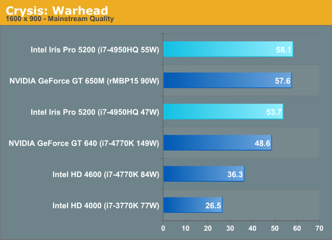
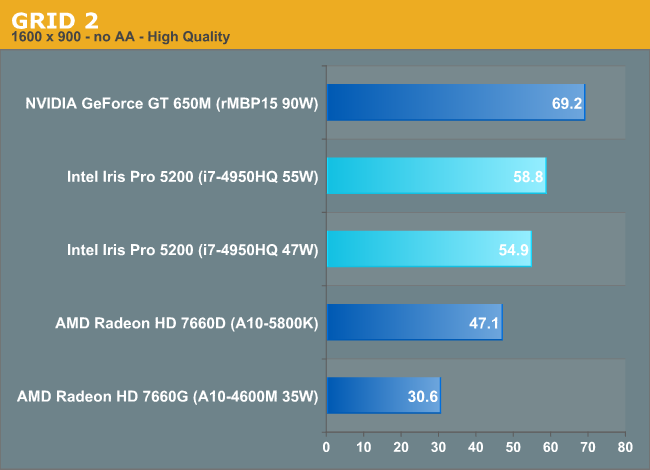
Why do you believe Iris Pro is benchmarked at 900p?

55294.png


55296.png


or even at lower 768p resolution?

Iris-Pro-Battlefield-3.png
 
Last edited:

insertcarehere

Senior member
Jan 17, 2013
639
607
136
The problem is the e-vram needs to be expanded and scaled as well, 128mb is peanuts once you get to real gaming and not a synthetic bench like 3dmark. What happens when textures take up 2gb vram? Iris is resorting to system ram for that and again, performance would tank hard.

So no, its not a simple matter of scaling up, it would have to be redesigned to take advantage of GDDR5, which then needs its own MC, there's no indications Intel can do a 7Gbps GDDR5 MC anytime soon.. or even if they could, it would add to the die space.

Once MS and Sony decided on a SoC design, there's no viable alternative but to go with AMD.

Considering that the xbone is using 32mb esram as a framebuffer, 128mb would have been very overkill for that purpose.
 

chernobog

Member
Jun 25, 2013
79
0
0
Becaused it has esram it does not mean it will be good for games. Only if find a way to use it but then its still more expensive than GDDR5 RAM and less things are stored, the framerate in games will skyrocket and crashing on Xbox One when not properly used in certain intensive scenarios... 100 fps and down to 1 fps.

Iris and Iris Pro are amazingly better but still way expensive and power hungry, not as efficient as GCN or GK104
 

DominionSeraph

Diamond Member
Jul 22, 2009
8,391
31
91
The problem is the e-vram needs to be expanded and scaled as well, 128mb is peanuts once you get to real gaming and not a synthetic bench like 3dmark. What happens when textures take up 2gb vram? Iris is resorting to system ram for that and again, performance would tank hard.

*cough* 32MB eSRAM...
 

ShintaiDK

Lifer
Apr 22, 2012
20,378
145
106
That 32mb eSRAM is for cache, the textures is loaded onto the 8gb system ddr3. Also don't forget: HSA custom SoC vs Intel iGPU.. no need to cough too hard.

Also, PS4 has GDDR5. Not sure why MS went retarded with DDR3 system ram..

The consoles dont support HSA.
 

Vesku

Diamond Member
Aug 25, 2005
3,743
28
86
Yes, the console chips were designed before even a preliminary HSA spec was presented. But the PS4 is said to have quite a bit of CPU+GPU integration, to the point of having an extra CPU<->GPU interconnect on top of the CPU<->RAM and GPU<->RAM.
 

insertcarehere

Senior member
Jan 17, 2013
639
607
136
That 32mb eSRAM is for cache, the textures is loaded onto the 8gb system ddr3. Also don't forget: HSA custom SoC vs Intel iGPU.. no need to cough too hard.

Also, PS4 has GDDR5. Not sure why MS went retarded with DDR3 system ram..

In MS's defense, Sony got lucky with high density GDDR5 chips, as everybody expected PS4 to be announced with only 4GB of ram. I also suspect the decision to go with 8GB GDDR5 probably will cost quite a bit for sony in the long run, I read somewhere that the cost of memory per PS4 would be around $100, and would be more difficult to reduce costs through process shrinks than MS's solution.
 

Exophase

Diamond Member
Apr 19, 2012
4,439
9
81
To all the people telling me Intel wouldn't sell it for low enough, wouldn't allow customization, would be sole source etc, I get it.. I'm not arguing against any of this stuff. Just exploring whether or not Intel has the capability to scale their IGP to remotely console competitive level while still in a feasible die size.

By all means Exophase. Come on. The 80eu is an unrealistic stretch also. Consoles plays real games and need consistent performance and keeping programming cost down. We are in the real world where there is no 3D mark. You need to go for the 100-120EU to get just reasonable power numbers and cost for the programming, and then you are already in what is borderline technical possible or at least technical reasonable imho. It just doesnt make technical sense in my world. And 100% economic impossible looking at the alternatives from NV or AMD - this is not a perhaps (or roi bracket for that matter).

Could you please draw your conclusion from some kind of benchmark comparison? I know it's hard since no one is benching stuff at the same resolution HD 5200 was benched at but I'm sure it could be done.

Then there is the question of the DDR5 controller - if chosen. As it have taken years for AMD and NV to get an efficient controller, - just look the gains from Keplar when NV fixed the memory issue, - i think its fair to assume, that if Intel was to chose and able to build an DDR5 controller - it wouldnt have the nessesary efficiency leaving the edram as the only viable option.

I think you overestimate the domain-specific knowledge necessary to get an efficient GDDR5 controller once you have an efficient DDR3 controller.

And doubling the iris pro ram here is also a stretch - leaving 3 og 4 times the size as the possible solution (edit saw silverforce beat me to it).

Why would you even need the 128MB in Crystalwell when XBox One only uses 32MB? Much less three or four times that.. doesn't make any sense to me. Intel themselves suggest 128MB is overkill.

At the same time two Haswell cores just dont cut it. It dont, its not a perhaps. For the simple reason that the new consoles is build as heavy multitasking entertainment machines. Its a requirement, leaving 4 cores as the only option because you need human beeings to program for the consoles and get paid doing it.

I don't really agree with this. 2C4T Haswell at > 3.5GHz is pretty competitive with 8C 1.6GHz Jaguar in aggregate throughput before you even consider scaling overhead, especially if we're talking SIMD heavy code that is often what a lot of console code ends up as. With each Haswell core having 2x256-bit FP + integer, including FMA, it can easily keep up there.