The real reasons Microsoft and Sony chose AMD for consoles [F]

Page 7 - Seeking answers? Join the AnandTech community: where nearly half-a-million members share solutions and discuss the latest tech.

Charles Kozierok

Elite Member
May 14, 2012
6,762
1
0
There is one link in my OP that explains why Intel was rejected

Which, as mentioned repeatedly, does not mean that Intel could not produce a custom SoC, just that they did not offer to do so.

At the other side, all the posters claiming here that Intel could do it if it was interested have not backed up their ridiculous claims.

That's not how reasonable argumentation works. It is incumbent on the ones proferring specific claims to support them. You and others are stating flatly that Intel was technologically incapable of producing this chip. I and others are saying that this is possible, but that we do not have sufficient knowledge of the contract requirements to know.

My position is neutral; your position makes a positive assertion that is unsupported by the evidence.
 

3DVagabond

Lifer
Aug 10, 2009
11,951
204
106
There's no requirement for an APU. If Sony or Microsoft could've gotten an i7 and 7970M or 680M for the same price, do you think they would've rejected it because, "OMGZ its not on the same package"? Gaming laptops have been using discrete graphics for over a decade, so I think a console 3x the size could handle it.

Don't kid yourself. Discrete was always on the table. But Intel had no reason to play. Intel has an image worth billions in the business world, and consoles are for casuals. It'd be like Abercrombie & Fitch giving out their clothes to the homeless.
The homeless can wear Sears.

There's very little profit in console hardware, and you open yourself up to having your name attached to tons of bad press if the console doesn't do well, with no corresponding good press if it's great.
If Intel can take a Xeon die, disable the ECC, hyperthreading, virtualization, and 2MB of cache, call it an "i5", and still make a huge profit on it, I somehow think their die space is worth a little more than cost. AMD, OTOH, paid a couple hundred million dollars for nothing rather than take their own chips.

AMD haters like to present the argument that it's only because AMD is willing to work for less than anyone else that they got the contract. Unless someone can back that up with something solid, it sounds like little else but sour grapes, I'm afraid. Intel could walk on water, but it doesn't mean they could offer a competitive package to what AMD did. All of their CPU accomplishments mean little if they can't package it with a competitive GPU as well, which is very absent in your list of Intel accomplishments.

Have you seen anywhere that Intel or nVidia ever offered up any kind of hardware at any kind of price?
 

blackened23

Diamond Member
Jul 26, 2011
8,548
2
0
It's completely worthless to ask for evidence when everyone in this thread knows well that no such evidence is made public. Ever. Asking for iron clad evidence for talks that happened behind closed doors and is 100% confidential isn't going to happen.

The only two viable options, given that MS and Sony wanted:

1) x86
2) ease of development
3) SOC

Leaves intel and AMD as the only contenders to meet this requirement, with ARM, nvidia, and MIPs not able to meet it. All ARM SOCs were not in consideration as they are, for all intents and purposes, extremely low performance but high efficiency chips. Until ARM SOCs can provide 64 bit and high performance, they will not appear in high performance devices. Nvidia could only provide a low performance ARM SOC or a discrete GPU but that would not meet the SOC requirement as nvidia cannot provide x86 (they do not have an x86 license). Intel could obviously have made an SOC, why didn't they? Nobody knows. We do know that MS was unhappy with their prior arrangement with intel with the original xbox, but again, asking for concrete evidence when EVERYONE in this thread knows that isn't possible is a complete waste of time.

In short, it wasn't a technical issue. Intel could well have designed such a SOC to meet all of the requirements. Why didn't they? We'll never know. That being said, with the AMD solution providing near 2Tflops of performance will still be substantially better than prior generation consoles, by a factor of 10 at least.
 
Last edited:

3DVagabond

Lifer
Aug 10, 2009
11,951
204
106
It's completely worthless to ask for evidence when everyone in this thread knows well that no such evidence is made public. Ever. Asking for iron clad evidence for talks that happened behind closed doors and is 100% confidential isn't going to happen.

The only two viable options, given that MS and Sony wanted:

1) x86
2) ease of development
3) SOC

Leaves intel and AMD as the only contenders to meet this requirement. Nvidia could only provide a low performance ARM SOC or a discrete GPU but that would not meet the SOC requirement as nvidia cannot provide x86 (they do not have an x86 license). Intel could obviously have made an SOC, why didn't they? Nobody knows. We do know that MS was unhappy with their prior arrangement with intel with the original xbox, but again, asking for concrete evidence when EVERYONE in this thread knows that isn't possible is a complete waste of time.

What would Intel provide on the GPU side? What do they have that could approach 1100 GCN2.0 shader cores?
 

blackened23

Diamond Member
Jul 26, 2011
8,548
2
0
What would Intel provide on the GPU side? What do they have that could approach 1100 GCN2.0 shader cores?

Just like the Jaguar core, the GT3 graphics core is highly scalable - it can go from extremely low performance to extremely high performance depending on the configuration and number of streaming processors used. This is not different than the Jaguar graphics core - it can be designed for low performance tablet devices, or it can be scaled to near 7970M performance in a dedicated set top device. Again - scalable architecture -- Intel just hasn't done it as they have strict TDP requirements with their HD5000/GT3 graphics, since the target market is designed for AIOs and highly mobile devices.

That being said, it has always seemed to me that intel has done exceptionally well in synthetic benchmarks but gaming performance seems awry in comparison to mobile discrete GPUs. For instance, the GT3 exceeds the 650M in most synthetics, while the 650M is actually faster in many games. So I don't know how to explain that. The point remains however, that there was no technical issue with using intel for a SOC. Why they weren't used will remain a mystery, however.
 
Last edited:

3DVagabond

Lifer
Aug 10, 2009
11,951
204
106
Just like the Jaguar core, the GT3 graphics core is highly scalable - it can go from extremely low performance to extremely high performance depending on the configuration and number of streaming processors used. This is not different than the Jaguar graphics core - it can be designed for low performance tablet devices, or it can be scaled to near 7970M performance in a dedicated set top device. Again - scalable architecture -- Intel just hasn't done it as they have strict TDP requirements with their HD5000/GT3 graphics, since the target market is designed for AIOs and highly mobile devices.

That being said, it has always seemed to me that intel has done exceptionally well in synthetic benchmarks but gaming performance seems awry in comparison to mobile discrete GPUs. For instance, the GT3 exceeds the 650M in most synthetics, while the 650M is actually faster in many games. So I don't know how to explain that. The point remains however, that there was no technical issue with using intel for a SOC. Why they weren't used will remain a mystery, however.

Just so I'm understanding you... You are saying that Intel could compete with AMD (and I guess nVidia too) in graphics performance, but simply choose not to? :\
 

blackened23

Diamond Member
Jul 26, 2011
8,548
2
0
Just so I'm understanding you... You are saying that Intel could compete with AMD (and I guess nVidia too) in graphics performance, but simply choose not to? :\

Yes, I'm saying that intel could have provided a SOC solution for a console but whatever reason didn't, and we'll never know why. Again, the requirements presented by sony and MS were for an x86 SOC. Only intel or AMD could have made such a device. Nvidia was not in the running due to the lack of an x86 license - obviously that would prevent them from making an x86 SOC.
 

3DVagabond

Lifer
Aug 10, 2009
11,951
204
106
Yes, I'm saying that intel could have provided a SOC solution for a console but whatever reason didn't, and we'll never know why. Again, the requirements presented by sony and MS were for an x86 SOC. Only intel or AMD could have made such a device.

I guess we'll just have to disagree on this point. When I see Intel produce a GPU or iGPU that competes in performance to AMD I'll accept they could have offered a competing design to Sony/M$. Until then I think it's just wishful thinking.
 

jpiniero

Lifer
Oct 1, 2010
14,616
5,227
136
AMD haters like to present the argument that it's only because AMD is willing to work for less than anyone else that they got the contract.

I guess we won't know for sure until AMD reports financials after the consoles launch, but AMD has been crowing about the revenue it's going to bring in while conveniently ignoring the margin issue. That's just how AMD rolls.

It could be very useful in dealing with the WSA though.
 

DominionSeraph

Diamond Member
Jul 22, 2009
8,391
31
91
AMD haters like to present the argument that it's only because AMD is willing to work for less than anyone else that they got the contract. Unless someone can back that up with something solid, it sounds like little else but sour grapes, I'm afraid.

Intel made $4.5 billion profit in the last two quarters.
AMD lost $619 million.

AMD's grapes don't look very sweet to me.

Unless you can show Intel losing out business to console hardware, sounds like you don't even know which tree holds Intel's billions in grapes.
 
Last edited:

Erenhardt

Diamond Member
Dec 1, 2012
3,251
105
101
Just like the Jaguar core, the GT3 graphics core is highly scalable - it can go from extremely low performance to extremely high performance depending on the configuration and number of streaming processors used. This is not different than the Jaguar graphics core - it can be designed for low performance tablet devices, or it can be scaled to near 7970M performance in a dedicated set top device. Again - scalable architecture -- Intel just hasn't done it as they have strict TDP requirements with their HD5000/GT3 graphics, since the target market is designed for AIOs and highly mobile devices.

Ohhh my... Look how far have you sailed into the wonderland.

The Crystalwell die measures 7mm x 12mm (84mm^2), while the quad-core Haswell + GT3 die is a whopping 264mm^2 (16.2mm x 16.3mm). Working backwards from the official data Intel provided (177mm^2 for quad-core GT2), I came up with an 87mm^2 adder for the extra hardware in Haswell GT3 vs. GT2. Doubling that 87mm^2 we get a rough idea of how big the full 40 EU Haswell GPU might be: 174mm^2. If my math is right, this means that in a quad-core Haswell GT3 die, around 65% of the die area is GPU. This is contrary to the ~33% in a quad-core Haswell GT2. I suspect a dual-core + GT3 design is at least half GPU.
40EU = 174mm^2@22nm = 832 GFLOPS = 10.4 GPixels/s = 20.8 GTexels/s
14CU = 160mm^2@28nm = 1792 GFLOPS = 17.2 GPixels/s = 60.2 GTexels/s

And we will just leave iris pro gaming performance under GT640 level without any comment.
To match 14CU (hd7790)on paper, they would need at least 80EU, which will be 300+mm^2 - about the size of 7970 core.

GT3 graphics is bad no matter how you look at it.
Performance/mm^2 is bad, and performance/transistor is terrible.
 

zlatan

Senior member
Mar 15, 2011
580
291
136

They are far away from reality. One of the main claim for the next gen is the support for unified virtual memory. The truth is that AMD was the only company who undertook the task to build such a complex chip for the next gen consoles before 2014. There are several other company who've also expressed an interest for a design win, but they simply can't offer an architectural integration before 2015 or 2016.
Basically AMD was the only company who have accepted the Sony/MS tender, and this is why the new consoles based on the same architecture.
 
Aug 11, 2008
10,451
642
126
I guess we'll just have to disagree on this point. When I see Intel produce a GPU or iGPU that competes in performance to AMD I'll accept they could have offered a competing design to Sony/M$. Until then I think it's just wishful thinking.

HD 4600 is not far behind A10 on the desktop and the high end mobile solutions are faster than anything amd produces. So on performance they definitely have the ability to "compete". Price is another issue however.
 

AnandThenMan

Diamond Member
Nov 11, 2004
3,949
504
126
Don't kid yourself. Discrete was always on the table. But Intel had no reason to play. Intel has an image worth billions in the business world, and consoles are for casuals. It'd be like Abercrombie & Fitch giving out their clothes to the homeless.
The homeless can wear Sears.
wow.
 

Vesku

Diamond Member
Aug 25, 2005
3,743
28
86
Yes, I'm saying that intel could have provided a SOC solution for a console but whatever reason didn't, and we'll never know why. Again, the requirements presented by sony and MS were for an x86 SOC. Only intel or AMD could have made such a device. Nvidia was not in the running due to the lack of an x86 license - obviously that would prevent them from making an x86 SOC.

Sure they could put enough EUs on a chip to at least get synthetic performance to 7790 or 7870 level but how many EUs would that take, how much power would it need, and how much would it cost?

My hunch is the answer to all those questions is: A lot.

Feel free to extrapolate from the eDRAMless 4600->5100.
 

ThePeasant

Member
May 20, 2011
36
0
0
It doesn't seem like anyone here has any kind of inside information on the details of the negotiations or any contracts involved in bringing these consoles to market. So why then then do some complain about a lack of evidence disparaging Intel's ability to provide a console class GPU - taken by some to mean that since we don't know that they can't then clearly they are able to since they are Intel, but others still (who presumably also have no clue about any negotiations) proclaim the only reason AMD got the contract is because they settled on low margins.

Granted Intel has made some impressive strides (considering their history) lately, we shouldn't pretend like Intel is currently a name in high performance graphics. I certainly believe Intel could make a high performance GPU, but at the expense of die size/power consumption relative to AMD.

My opinion is that cost was but one factor among many, and that AMD's history of high performance GPUs, their x86 licence and product timing were probably factors as well.
 
Jun 8, 2013
40
0
0
HD 4600 is not far behind A10 on the desktop and the high end mobile solutions are faster than anything amd produces. So on performance they definitely have the ability to "compete". Price is another issue however.

It's on average 30% slower than desktop Richland which on the GPU front brought no noticeable improvements over Trinity. Desktop Trinity was launched some 9 months before HD 4600.
 

insertcarehere

Senior member
Jan 17, 2013
639
607
136
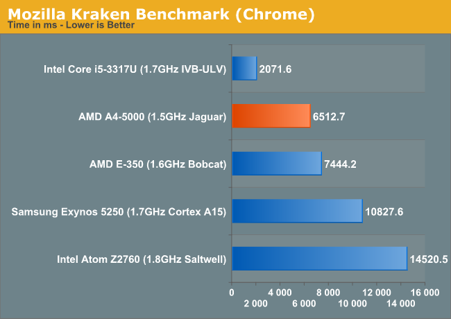
Uhh what? What makes you think this? Bobcat was quicker than A15 cores, and Jaguar is alot quicker than Bobcat.

Explain?

First graph I could find:

54812.png


Edit: Aah that Samsung is a dual core arm soc. Nevermind.

I would not use a browser-based benchmark as a very valid benchmark across different OSes.

40EU = 174mm^2@22nm
Considering we already know that the dual core GT3 part is 181mm^2, I think the gpu would be in the ballpark of 95-105mm^2, which would be plenty big by itself. (cape verde size on 28nm)
 
Last edited:

Keysplayr

Elite Member
Jan 16, 2003
21,209
50
91
There is one link in my OP that explains why Intel was rejected:


At the other side, all the posters claiming here that Intel could do it if it was interested have not backed up their ridiculous claims. Let me be clear I have provided one link, they (including you in the message that I replied) have provided zero links.

What you quoted does not show Intel offering anything. To be honest, I don't think they ever did. And you're asserting that Intel does not have the technological capability to produce a SoC for a console is a farce. A big one.
 

Exophase

Diamond Member
Apr 19, 2012
4,439
9
81
40EU = 174mm^2@22nm = 832 GFLOPS = 10.4 GPixels/s = 20.8 GTexels/s

There's something seriously inconsistent with the reasoning here:

http://www.anandtech.com/show/6993/intel-iris-pro-5200-graphics-review-core-i74950hq-tested/4

Dual core GT3 Haswell is 181mm^2 and has that same 40EUs. The two CPU cores, uncore, L3 cache, so on and so forth would be only 7mm^2 which can't possibly be the case. I don't know why the GT3e die is so big but it can't be strictly due to the 40EUs.

Based on the die shot here:

http://download.intel.com/newsroom/...h_Generation_Intel_Core_Dual_Core_Hero_HR.jpg

It looks like the full GPU is around 102mm^2. So a full 2x equivalent part would be 283mm^2. For consoles you'd also need more memory controllers and either change them to GDDR5 (which Intel has no experience with AFAIK, could be a bad idea) or a separate bus for Crystalwell style eDRAM (while that could be what's taking a big chunk of the GT3e die area it really shouldn't be); you'd also need a fundamentally higher bandwidth solution than what Iris HD 5200 employs. But you can balance this against a smaller L3 cache requirement; 2-3MB should be sufficient. You'd still have something that's probably larger than the APU Sony's using, but not necessarily so large as to be intractable - maybe ~350mm^2 is doable. Probably not as large as MS's chip if it's really 400mm^2, but it would be putting the extra memory pool off chip so not a great comparison.
 
Last edited:
Mar 10, 2006
11,715
2,012
126
There's something seriously inconsistent with the reasoning here:

http://www.anandtech.com/show/6993/intel-iris-pro-5200-graphics-review-core-i74950hq-tested/4

Dual core GT3 Haswell is 181mm^2 and has that same 40EUs. The two CPU cores, uncore, L3 cache, so on and so forth would be only 7mm^2 which can't possibly be the case. I don't know why the GT3e die is so big but it can't be strictly due to the 40EUs.

Based on the die shot here:

http://download.intel.com/newsroom/...h_Generation_Intel_Core_Dual_Core_Hero_HR.jpg

It looks like the full GPU is around 102mm^2. So a full 2x equivalent part would be 283mm^2. For consoles you'd also need more memory controllers and either change them to GDDR5 (which Intel has no experience with AFAIK, could be a bad idea) or a separate bus for Crystalwell style eDRAM (while that could be what's taking a big chunk of the GT3e die area it really shouldn't be); you'd also need a fundamentally higher bandwidth solution than what Iris HD 5200 employs. But you can balance this against a smaller L3 cache requirement; 2-3MB should be sufficient. You'd still have something that's probably larger than the APU Sony's using, but not necessarily so large as to be intractable - maybe ~350mm^2 is doable. Probably not as large as MS's chip if it's really 400mm^2, but it would be putting the extra memory pool off chip so not a great comparison.

Exophase,

Intel's Xeon Phi uses GDDR5.
 

Erenhardt

Diamond Member
Dec 1, 2012
3,251
105
101
There's something seriously inconsistent with the reasoning here:

http://www.anandtech.com/show/6993/intel-iris-pro-5200-graphics-review-core-i74950hq-tested/4

Dual core GT3 Haswell is 181mm^2 and has that same 40EUs. The two CPU cores, uncore, L3 cache, so on and so forth would be only 7mm^2 which can't possibly be the case. I don't know why the GT3e die is so big but it can't be strictly due to the 40EUs.
Based on this:
http://www.anandtech.com/show/6993/intel-iris-pro-5200-graphics-review-core-i74950hq-tested/4

Going from 4 cores and 20EUs to 2 cores and 40EUs increased die size, which means 20EUs take more place than 2 cores. If it is true, then the gpu takes the bigger part of the 4 core, 40EUs chip.

GT3e eDRAM have its own dedicated 84mm^2 of silicon.
 
Mar 10, 2006
11,715
2,012
126
Guys, the reason the GT3e die is so large is that it's done in the name of power efficiency. You want more performance at less power? Go ultra parallel, clock lower.

If your power budget is bigger, then you can clock way higher to save on die space.