The new AMD Picasso APU appears in the UserBenchmark database

Page 2 - Seeking answers? Join the AnandTech community: where nearly half-a-million members share solutions and discuss the latest tech.

AtenRa

Lifer
Feb 2, 2009
14,000
3,357
136
Aren't the same masks. Way too many changes on the process front to just copy paste the masks. The fin shape changed, the eSiGe trenches are buried deeper, etc'

AMD saved money on reworking the die with the new libraries, but they still had to make new masks.

If they changed all that, then they would need new masks for both FEOL and BEOL process.
 

PeterScott

Platinum Member
Jul 7, 2017
2,605
1,540
136
I dont believe they can use the same masks from 14nm to 12nm.

There is an interview with someone from GF talking about "12nm", saying there were two options. Doing a new tapeout and getting the actual dimensional changes, or reusing the same design and just get a some process tweaks, and the specifically mentioned AMD WRT the latter.

Pinnacle Ridge has been measured with micrometers to find that it is the exact same size as the Summit Ridge.

IMO there is enough evidence that PR is just some process tweaks on the same Tapeout/Masks and is thus a Major cost savings, over doing a new tapeout/Masks.
 
  • Like
Reactions: french toast

CatMerc

Golden Member
Jul 16, 2016
1,114
1,149
136
There is an interview with someone from GF talking about "12nm", saying there were two options. Doing a new tapeout and getting the actual dimensional changes, or reusing the same design and just get a some process tweaks, and the specifically mentioned AMD WRT the latter.

Pinnacle Ridge has been measured with micrometers to find that it is the exact same size as the Summit Ridge.

IMO there is enough evidence that PR is just some process tweaks on the same Tapeout/Masks and is thus a Major cost savings, over doing a new tapeout/Masks.
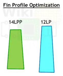
You can't just reuse the same masks to print features that weren't there before. The Wikichip article showed differences that simply don't allow such a thing. The fin shape itself changed.

vlsi_2018_12lp_fin_profile-246x300.png


Pinnacle Ridge is the same layout as Summit Ridge, but that still requires new masks. Just not much work other than that. Like hitting compile with the new PDK on the existing design. To get size benefits they'd need to go in there and put 7.5T cells where it makes sense to do so.
 
  • Like
Reactions: Abwx

PeterScott

Platinum Member
Jul 7, 2017
2,605
1,540
136
You can't just reuse the same masks to print features that weren't there before. The Wikichip article showed differences that simply don't allow such a thing. The fin shape itself changed.

vlsi_2018_12lp_fin_profile-246x300.png


Pinnacle Ridge is the same layout as Summit Ridge, but that still requires new masks. Just not much work other than that. Like hitting compile with the new PDK on the existing design. To get size benefits they'd need to go in there and put 7.5T cells where it makes sense to do so.

I am betting the did not spend tens of millions of dollars on new masks for such an inconsequential change. The changes of PR are what you can expect on mere process refinement for a process in production for a year.
 
  • Like
Reactions: NTMBK

CatMerc

Golden Member
Jul 16, 2016
1,114
1,149
136
I am betting the did not spend tens of millions of dollars on new masks for such an inconsequential change. The changes of PR are what you can expect on mere process refinement for a process in production for a year.
The natural improvements were already implemented... 14nm has been in production for a long while now, and it can mostly clearly be seen from RX 480 to RX 580. There's no way what we are seeing with Pinnacle Ridge is normal process improvement.

If it means increasing sales for another year while waiting on the new design, a relatively small investment in the masks is worth it. It's the engineering time that's really costly, and it there wasn't a lot poured into Pinnacle.
 

PeterScott

Platinum Member
Jul 7, 2017
2,605
1,540
136
Really, all I see in PR is a small bit of clock speed boost indicating cleaner signals. Everything else is microcode updates to take advantage of that.

The costs I have seen for a complete set of masks at 14nm, was > 50 Million Dollars. You don't spend 50 million dollars to remask the the exact same chip, at the exact same size/function, just for a very tiny clock speed bump.

Pinnacle Ridge is Process improvement (same Masks) + microcode enhancement that benefit from it.

If Picasso is "12nm" it will be the same thing.
 
  • Like
Reactions: NTMBK

maddie

Diamond Member
Jul 18, 2010
4,723
4,628
136
Really, all I see in PR is a small bit of clock speed boost indicating cleaner signals. Everything else is microcode updates to take advantage of that.

The costs I have seen for a complete set of masks at 14nm, was > 50 Million Dollars. You don't spend 50 million dollars to remask the the exact same chip, at the exact same size/function, just for a very tiny clock speed bump.

Pinnacle Ridge is Process improvement (same Masks) + microcode enhancement that benefit from it.

If Picasso is "12nm" it will be the same thing.
Who says you need a complete set of masks? AMD specifically stated that they did not take advantage of the available increased density and I take this to mean that the back end is the same, but the fin level is changed.
 

PeterScott

Platinum Member
Jul 7, 2017
2,605
1,540
136
Who says you need a complete set of masks? AMD specifically stated that they did not take advantage of the available increased density and I take this to mean that the back end is the same, but the fin level is changed.

I wish I could find the GF interview I read, that stated what was happening. This was back before Ryzen 2xxxx was released, the GF speaker, basically said AMD was not doing a new tape-out and was taking advantage of process improvements.

Given what I read and the outcome we have seen (small clock speed boost, same exact die size) it really is the logical outcome that this is just a a process tweak.

If you want to argue they partially tweaked a couple of masks, for marginal costs; Fine. But that's effectively the same thing. We will never know exactly to the dollar amount they spent on the upgrade.

The issue is they didn't do anything like the cost full set of masks, and they have chip of the exact same dimensions, and exact same units, performing just a small amount better.

It is exactly the kind of smart tweaking, low cost move AMD needs to be making, to extend the life a of design, and boost profit.

If another generation 12nm APU appears, it would be logical to expect this exact same kind of change.

The new design and new tapeout for the APU will be reserved for Zen2 architecture and 7nm process.

Tying this back to the original post. If there is another APU showing up online somewhere this early, chances are it is 12nm process tweak, and not the new 7nm Zen 2 core based design.
 
  • Like
Reactions: beginner99

maddie

Diamond Member
Jul 18, 2010
4,723
4,628
136
I wish I could find the GF interview I read, that stated what was happening. This was back before Ryzen 2xxxx was released, the GF speaker, basically said AMD was not doing a new tape-out and was taking advantage of process improvements.

Given what I read and the outcome we have seen (small clock speed boost, same exact die size) it really is the logical outcome that this is just a a process tweak.

If you want to argue they partially tweaked a couple of masks, for marginal costs; Fine. But that's effectively the same thing. We will never know exactly to the dollar amount they spent on the upgrade.

The issue is they didn't do anything like the cost full set of masks, and they have chip of the exact same dimensions, and exact same units, performing just a small amount better.

It is exactly the kind of smart tweaking, low cost move AMD needs to be making, to extend the life a of design, and boost profit.

If another generation 12nm APU appears, it would be logical to expect this exact same kind of change.

The new design and new tapeout for the APU will be reserved for Zen2 architecture and 7nm process.

Tying this back to the original post. If there is another APU showing up online somewhere this early, chances are it is 12nm process tweak, and not the new 7nm Zen 2 core based design.
You have it wrong.

CatMerc said that there were transistor improvements necessitating new masks.

First you said:
The costs I have seen for a complete set of masks at 14nm, was > 50 Million Dollars. You don't spend 50 million dollars to remask the the exact same chip, at the exact same size/function, just for a very tiny clock speed bump.

I said:
Who says you need a complete set of masks? AMD specifically stated that they did not take advantage of the available increased density and I take this to mean that the back end is the same, but the fin level is changed.

Now you say:
The issue is they didn't do anything like the cost full set of masks, and they have chip of the exact same dimensions, and exact same units, performing just a small amount better.

Pinnacle Ridge is Process improvement (same Masks) + microcode enhancement that benefit from it.


The transistors have changed but the interconnects between the functional units are the same. I think you believe that because the microarchitecture is identical, that means that its all the same.
Notice how you keep stressing "the exact same chip".

How do you end up with more dark silicon and taking up less space, by keeping everything the same? Please tell me.


Here is the relevant info from the Anandtech 2700X review.
https://www.anandtech.com/print/12625/amd-second-generation-ryzen-7-2700x-2700-ryzen-5-2600x-2600

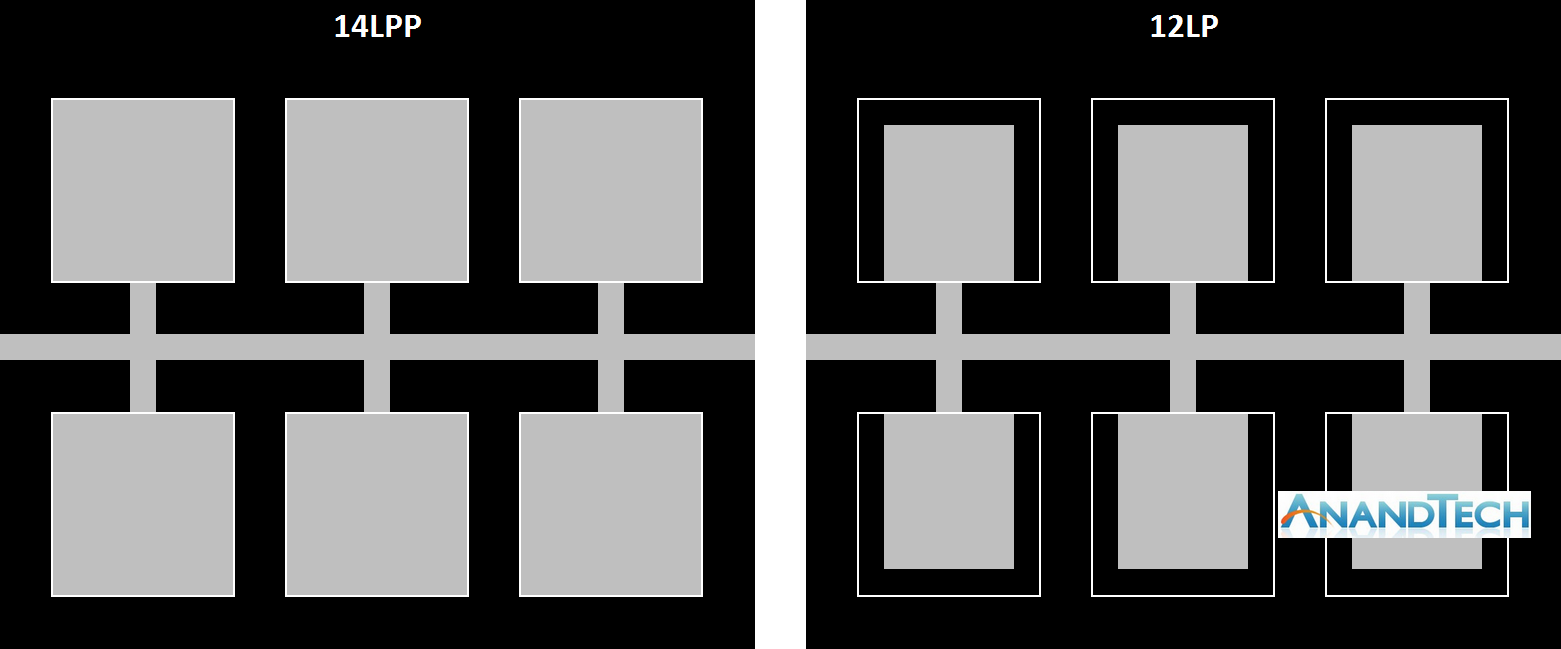
"One interesting element is that although GF claims that there is a 15% density improvement, AMD is stating that these processors have the same die size and transistor count as the previous generation. Ultimately this seems in opposition to common sense – surely AMD would want to use smaller dies to get more chips per wafer?

Ultimately, the new processors are almost carbon copies of the old ones, both in terms of design and microarchitecture. AMD is calling the design of the cores as ‘Zen+’ to differentiate them to the previous generation ‘Zen’ design, and it mostly comes down to how the microarchitecture features are laid out on the silicon. When discussing with AMD, the best way to explain it is that some of the design of the key features has not moved – they just take up less area, leaving more dark silicon between other features.
12nm.png

Here is a very crude representation of features attached to a data path. On the left is the 14LPP design, and each of the six features has a specific size and connects to the bus. Between each of the features is the dark silicon – unused silicon that is either seen as useless, or can be used as a thermal buffer between high-energy parts. On the right is the representation of the 12LP design – each of the features have been reduced in size, putting more dark silicon between themselves (the white boxes show the original size of the feature). In this context, the number of transistors is the same, and the die size is the same. But if anything in the design was thermally limited by the close proximity of two features, there is now more distance between them such that they should interfere with each other less.
 
  • Like
Reactions: french toast

Vattila

Senior member
Oct 22, 2004
799
1,351
136
Here is a very crude representation of features attached to a data path.

I'll quote seemingly knowledgeable Reddit user KKMX: "This isn't good. That image is very wrong. By using the 14LPP 9T cells on 12LP, you get exactly the same thing as the original 14LPP. Nothing gets smaller because the features are identical (It's why Zen+ and Zen have the exact same die size). Actually, the whole description you quoted [from the AnandTech article] is terrifyingly incorrect. Yikes. Instead, the cells and the overall SoC benefits from the transistors improvements exclusively."

I doubt there is "dark silicon" anywhere. I think they simply redid the masks at the transistor layers to get the improved transistor and kept the other masks (metal layers) unchanged.

https://fuse.wikichip.org/news/1497/vlsi-2018-globalfoundries-12nm-leading-performance-12lp/
 

maddie

Diamond Member
Jul 18, 2010
4,723
4,628
136
I'll quote seemingly knowledgeable Reddit user KKMX: "This isn't good. That image is very wrong. By using the 14LPP 9T cells on 12LP, you get exactly the same thing as the original 14LPP. Nothing gets smaller because the features are identical (It's why Zen+ and Zen have the exact same die size). Actually, the whole description you quoted [from the AnandTech article] is terrifyingly incorrect. Yikes. Instead, the cells and the overall SoC benefits from the transistors improvements exclusively."

I doubt there is "dark silicon" anywhere. I think they simply redid the masks at the transistor layers to get the improved transistor and kept the other masks (metal layers) unchanged.

https://fuse.wikichip.org/news/1497/vlsi-2018-globalfoundries-12nm-leading-performance-12lp/
The bolded part is basically what I said a few post ago.

Quoting myself:
"Who says you need a complete set of masks? AMD specifically stated that they did not take advantage of the available increased density and I take this to mean that the back end is the same, but the fin level is changed."

The graphic is meant as a very basic explanatory tool and should not be taken literally, and I have to stress the following. This explanation came about in a discussion with AMD themselves. Who am I to know more than the designers. I'll certainly take their word than an unverified expert.

Quote from Anandtech article:
When discussing with AMD, the best way to explain it is that some of the design of the key features has not moved – they just take up less area, leaving more dark silicon between other features.
 

Vattila

Senior member
Oct 22, 2004
799
1,351
136
This explanation came about in a discussion with AMD themselves.

Misunderstandings in journalism is pretty common, I guess. According to Wikichip, process feature sizes for 12LP and 14LPP are exactly the same. If so, the only way to get any density advantage is to use the 7.5T standard cell library (fewer tracks per standard cell, i.e. fewer metal tracks and fewer fins per transistor in each cell), and they did not (they stuck with 9T).

GlobalFoundries 12nm vs 14nm
14LPP (HP) 12LP (HP, HD) Δ
Fin Pitch
48 nm 48 nm 1.0x
Poly Pitch 84 nm 84 nm 1.0x
Metal 2 64 nm 64 nm 1.0x

https://fuse.wikichip.org/news/1497/vlsi-2018-globalfoundries-12nm-leading-performance-12lp/

PS. For those that don't know, a standard cell library is "a collection of low-level electronic logic functions such as AND, OR, INVERT, flip-flops, latches, and buffers."

https://en.wikipedia.org/wiki/Standard_cell
 
Last edited:
  • Like
Reactions: french toast

NostaSeronx

Diamond Member
Sep 18, 2011
3,683
1,218
136
GlobalFoundries:
Implemented a BKM for 15%+ device improvement (used for AMD Ryzen 2)
---
It should be noted that 12LP is a superset of 14nm/14nm+. To not use the new standard features AMD is essentially just using 14nm++.

12LP standardizes:

- SDB -> Single Diffusion Break, DDB -> Double Diffusion Break, CNRX -> Continuous RX
// Middle of Line Constructs and Continuous Rx (CNRX) that provided Best in Class PPAC in FDSOI and FinFET Technologies.
PPAC => Performance/Power/Area/Cost: CNRX is SDB density with DDB performance.
- Tungsten and Cobalt is introduced in 12LP Standard Libs
- There is the introduction of SRB/SiGe FinFETs in the High Performance option for 12LP, etc.
- 7.5-track with unknown Fin Depop.
- New fin structure, reductions for resistance/capacitance, etc.


14LPP 7.5T vs 12LP 7.5T:
https://www.bitsandchips.it/images/2017/01/28/glofo2.png
14LPP^
https://fuse.wikichip.org/wp-content/uploads/2018/07/vlsi_2018_12lp_75t_power_improvement.png
12LP^ // 84 CPP/9T vs 84 CPP/7.5T: AMD is 78 CPP/9T. So, AMD could in fact run both power and performance with 7.5T.

So, 12LP reduces power within the 0.5V and 0.7V volt range. With the new MOL/CNRX options available to 12LP based on the 22FDX/12FDX BKMs. 7.5T 12LP in higher voltages can possibly also have reduced power compared to 7.5T/9T 14LPP.

Pinnacle Ridge was a quick port and used none of this. As there was nothing wrong with Summit Ridge. However do the 7nm delay at AMD, Picasso will be slotted in the place of the 7nm DUV APU successor.

Synopsys (Jul 25, 2017):
307 GB/s aggregate bandwidth, which is 12 times the bandwidth of a DDR4 interface operating at 3200 Mb/s data rate. In addition, the DesignWare HBM2 IP solution delivers approximately ten times better energy efficiency than DDR4. Advanced graphics, high-performance computing (HPC) and networking applications are requiring more memory bandwidth to keep pace with the increasing compute performance brought by advanced process technologies.
-> https://i.imgur.com/js5vEWE.png

http://hexus.net/media/uploaded/2016/1/ba493ba3-2a6b-4fb4-a464-07c0f1006399.jpg
Onion 3 @ ~50 GB/s and HBM @ 128 GB/s for 2016 Raven Ridge.

https://www.overclock.net/photopost/data/1546548/e/ea/ea0d7e8a_AMD-socket-AM4-slides-12.jpeg
Bolded above appears here: APUs with Advanced Graphics in this September 2016 slide.

Bristol Ridge has double precision 2:1:
https://diit.cz/sites/default/files...9700_half_rate_dp_pcgh_pcgh.png?itok=UosmNHx9

Compare to Raven Ridge which doesn't:
https://www.aida64.com/sites/default/files/shot2_gpgpu_ravenridge.png

Picasso will not be using the same GFX revision as Raven Ridge. So, it is pretty much means that Picasso has a lot to catch up with.

Speculatively:
Picasso can be using ZenC(Fully Optimized 12LP "Zen+" CPU core) and VegaC(Fully Optimized 12LP "Vega+" GPU core).
With the inclusion of HBM2(die shrunk ver?) with enhanced[Full] Double Precision(64-bit) rate and Full rate Half(16-bit)/Quarter(8-bit). // Aquabolt (2.4 GHz HBM2- at Samsung/SK Hynix) has ULV modes for ~1.1V operation.
This in turn would push the ASP for the Performance APUs.

https://ark.intel.com/products/137979/Intel-Core-i7-8559U-Processor-8M-Cache-up-to-4_50-GHz
Recommend sold value: ~$431
AMD based on the CPU side converted to APU side would want an ASP of $220+.
If based on the not so good CPUs:
https://ark.intel.com/products/134903/Intel-Core-i9-8950HK-Processor-12M-Cache-up-to-4_80-GHz
Recommend sold value: ~$599
Then, like the CPU, AMD highest end APU would be sold for $299.

Don't even get me started with AMD's DTCO w/ GloFo for 14nm EUV(12LP+).
 
Last edited:
  • Like
Reactions: french toast

LightningZ71

Golden Member
Mar 10, 2017
1,627
1,898
136
So, I think the question is, will AMD use the same 12nm 9T process as they used for Zen+/Ryven 2X00 for Picasso, or will they use the denser 12nm 7.5T process for it? It appears that they are going to be making changes to the iGPU side of it from the above post, though I doubt anything else will be done to the core aside from microcode tweaks. If anything gets done to the actual circuits, the mask will have to change. If they are changing the mask at all, they would be somewhat foolish not to switch to the 7.5T process, especially on a processor that is first and foremost targeted at mobile applications. They advertised power/performance improvements on what is essentially a Raven Ridge architecture, 12nm 7.5T would seem to offer all of that.

I don't see HBM on a consumer APU product yet. Maybe on something for a console, but cost is certainly going to be a major factor there. Either way, a next gen console is going to have to be targeted at high end 4K and 8K televisions. I'm not sure that an APU with HBM2 is going to really cut the mustard there. Given how Sony and MS did sub generational upgrades to the PS4 and XBONE, an MCM with an 8 core ZEN+ with a VEGA derived chip and an HBM2 stack or 4 would definitely provide enough performance (the system RAM could be soldered on the board). Then, as Sony and MS introduce mid life upgrades for the console, they can simply use a newer MCM package revision as needed without having to touch any of the rest of the board.
 
  • Like
Reactions: William Gaatjes

moinmoin

Diamond Member
Jun 1, 2017
4,934
7,619
136
sa member climes RR has shared L2
That may well be true for all RR APUs (which are always only 1 CCX, so no inter CCX hops necessary).
For the record, he refers to following RR based Ryzen V1000 embedded product brief (page 4): https://www.amd.com/Documents/V1000-Family-Product-Brief.pdf
For comparison, the Zeppelin based Epyc 3000 embedded product brief makes only a single mention of shared L3 cache, none for L2: https://www.amd.com/Documents/3000-Family-Product-Brief.pdf
 

Gideon

Golden Member
Nov 27, 2007
1,608
3,573
136
This article somewhat mirrors my thoughts about Picasso. This strongly suggests that there will be no 7nm APU in 2019.

Raven Ridge was nice for getting the foot in the door. A 7nm Zen2 APU would truly disrupt the laptop market, while Intel is unable to get it's 10nm out (en-masse). 12nm won't really do the same, even if there are minor improvements and 7.5T cells used.

IMO for AMD a strong APU is the most important product after EPYC (market-share wise). Intel will get new products out in 2020 and AMD will lose that one huge opening.

At least I highly doubt Picasso will be a 1-1 shrink to 12nm so there is that. As RR already has most of the advancements of zen+, the difference would be negligible. It will most probably use 7.5T cells, and hopefully has better idle power-draw as well (maybe even lower power states?) as this is the weakest part of RR currently
 
  • Like
Reactions: neblogai

NTMBK

Lifer
Nov 14, 2011
10,208
4,940
136
This article somewhat mirrors my thoughts about Picasso. This strongly suggests that there will be no 7nm APU in 2019.

Raven Ridge was nice for getting the foot in the door. A 7nm Zen2 APU would truly disrupt the laptop market, while Intel is unable to get it's 10nm out (en-masse). 12nm won't really do the same, even if there are minor improvements and 7.5T cells used.

IMO for AMD a strong APU is the most important product after EPYC (market-share wise). Intel will get new products out in 2020 and AMD will lose that one huge opening.

At least I highly doubt Picasso will be a 1-1 shrink to 12nm so there is that. As RR already has most of the advancements of zen+, the difference would be negligible. It will most probably use 7.5T cells, and hopefully has better idle power-draw as well (maybe even lower power states?) as this is the weakest part of RR currently

When is EUV meant to be coming online? For a mass market low-margin part like a laptop processor, non-EUV 7nm might not be economical.
 

neblogai

Member
Oct 29, 2017
144
49
101
At least I highly doubt Picasso will be a 1-1 shrink to 12nm so there is that. As RR already has most of the advancements of zen+, the difference would be negligible. It will most probably use 7.5T cells, and hopefully has better idle power-draw as well (maybe even lower power states?) as this is the weakest part of RR currently

Another weak point is no LPDDR4 support. If Picasso is just 1-1 shrink- then no LPDDR4, and no premium 12-25W AMD portables. But if the die is redesigned- LPDDR4 support could possibly be added (LPDDR4 supporting memory controller was planned for Banded Kestrel for mid-2018 time frame).
 
  • Like
Reactions: Gideon

french toast

Senior member
Feb 22, 2017
988
825
136
Lpddr5 would be a great addition..100gb/s anyone?..would be available in Q3 2019 surely.
Full optical shrink of 12nm with 7.5T libraries, increase of CU to say 14..increase in idle power and a small bump to the clocks.
Good enough I think, disappointing no 7nm APU will be available though.
 

LightningZ71

Golden Member
Mar 10, 2017
1,627
1,898
136
Honestly, if all they did was a straight 12nm 7.5T shrink, and changed the DDR controller enough to support LPDDR4, they would have gone a long way to improving the penetration of the APU in the mid market. The shrink would improve the power/performance profile and LPDDR4 would reduce the total platform power demands. Both would go a long way to allowing the device to shrink while still providing the same performance, and to allow improved performance in existing form factors. With the lower power process, the manufacturers can use faster grades of RAM and more often use both channels while still hitting their power budget targets.
 
  • Like
Reactions: Vattila

AtenRa

Lifer
Feb 2, 2009
14,000
3,357
136
7nm volume is not enough to have all products in 2018-19.

First 7nm product is Radeon VEGA for servers = End of 2018. Low yields, low volume but high ASP
Then I believe it will be 7nm EPYC (1Q 2019 ?), again low yields, low volume but high ASP
Then 7nm Ryzen 3 Desktop (Q2 2019 ??), better yields, higher volume high ASP
After that in in Q4 2019 or Q1 2020 will get 7nm Ryzen 3 APUs. Higher yields, higher production volume, lower waffer cost (7nm one year+ in production)

Picasso at 12nm could get a nice 15% power drop with 5% higher Fmax, that will still be faster as a SOC against everything Intel has in 2019 at the same price points for Mobile.
 
  • Like
Reactions: french toast

moinmoin

Diamond Member
Jun 1, 2017
4,934
7,619
136
I still expect Picasso to test drive some new Zen 2 based tech and/or microcode while being based on the then more mature 12nm node Zen+ used, just like Raven Ridge does with the Zen+ improvements while using the more mature 14nm node. Timing wise having the yearly launch pattern apply for APUs as well, having RR early 2018, Picasso early 2019, and Renoir early 2020, sounds logical as well.
 

NTMBK

Lifer
Nov 14, 2011
10,208
4,940
136
I still expect Picasso to test drive some new Zen 2 based tech and/or microcode while being based on the then more mature 12nm node Zen+ used, just like Raven Ridge does with the Zen+ improvements while using the more mature 14nm node. Timing wise having the yearly launch pattern apply for APUs as well, having RR early 2018, Picasso early 2019, and Renoir early 2020, sounds logical as well.

It's going to use the Raven Ridge architecture. AMD have explicitly stated so. Don't expect any architectural improvements.
 
  • Like
Reactions: Olikan

moinmoin

Diamond Member
Jun 1, 2017
4,934
7,619
136
It's going to use the Raven Ridge architecture. AMD have explicitly stated so. Don't expect any architectural improvements.
Technically as far as we know RR didn't introduce architectural changes either, just microcode changes that used the existing architecture differently than the first Zeppelin chips did. We still don't have any details on what AMD intends to introduce as part of Zen 2.
 
  • Like
Reactions: Olikan