GlobalFoundries:
Implemented a BKM for 15%+ device improvement (used for AMD Ryzen 2)
---
It should be noted that 12LP is a superset of 14nm/14nm+. To not use the new standard features AMD is essentially just using 14nm++.
12LP standardizes:
- SDB -> Single Diffusion Break, DDB -> Double Diffusion Break, CNRX -> Continuous RX
// Middle of Line Constructs and
Continuous Rx (
CNRX) that provided Best in Class PPAC in FDSOI and FinFET Technologies.
PPAC => Performance/Power/Area/Cost: CNRX is SDB density with DDB performance.
- Tungsten and Cobalt is introduced in 12LP Standard Libs
- There is the introduction of SRB/SiGe FinFETs in the High Performance option for 12LP, etc.
- 7.5-track with unknown Fin Depop.
- New fin structure, reductions for resistance/capacitance, etc.
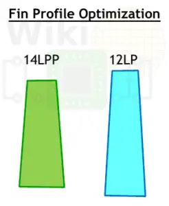
14LPP 7.5T vs 12LP 7.5T:
https://www.bitsandchips.it/images/2017/01/28/glofo2.png
14LPP^
https://fuse.wikichip.org/wp-content/uploads/2018/07/vlsi_2018_12lp_75t_power_improvement.png
12LP^ // 84 CPP/9T vs 84 CPP/7.5T: AMD is 78 CPP/9T. So, AMD could in fact run both power and performance with 7.5T.
So, 12LP reduces power within the 0.5V and 0.7V volt range. With the new MOL/CNRX options available to 12LP based on the 22FDX/12FDX BKMs. 7.5T 12LP in higher voltages can possibly also have reduced power compared to 7.5T/9T 14LPP.
Pinnacle Ridge was a quick port and used none of this. As there was nothing wrong with Summit Ridge. However do the 7nm delay at AMD, Picasso will be slotted in the place of the 7nm DUV APU successor.
Synopsys (Jul 25, 2017):
307 GB/s aggregate bandwidth, which is 12 times the bandwidth of a DDR4 interface operating at 3200 Mb/s data rate. In addition, the DesignWare HBM2 IP solution delivers approximately ten times better energy efficiency than DDR4.
Advanced graphics, high-performance computing (HPC) and networking applications are requiring more memory bandwidth to keep pace with the increasing compute performance brought by advanced process technologies.
->
https://i.imgur.com/js5vEWE.png
http://hexus.net/media/uploaded/2016/1/ba493ba3-2a6b-4fb4-a464-07c0f1006399.jpg
Onion 3 @ ~50 GB/s and HBM @ 128 GB/s for 2016 Raven Ridge.
https://www.overclock.net/photopost/data/1546548/e/ea/ea0d7e8a_AMD-socket-AM4-slides-12.jpeg
Bolded above appears here: APUs with Advanced Graphics in this September 2016 slide.
Bristol Ridge has double precision 2:1:
https://diit.cz/sites/default/files...9700_half_rate_dp_pcgh_pcgh.png?itok=UosmNHx9
Compare to Raven Ridge which doesn't:
https://www.aida64.com/sites/default/files/shot2_gpgpu_ravenridge.png
Picasso will not be using the same GFX revision as Raven Ridge. So, it is pretty much means that Picasso has a lot to catch up with.
Speculatively:
Picasso can be using ZenC(Fully Optimized 12LP "Zen+" CPU core) and VegaC(Fully Optimized 12LP "Vega+" GPU core).
With the inclusion of HBM2(die shrunk ver?) with enhanced[Full] Double Precision(64-bit) rate and Full rate Half(16-bit)/Quarter(8-bit). // Aquabolt (2.4 GHz HBM2- at Samsung/SK Hynix) has ULV modes for ~1.1V operation.
This in turn would push the ASP for the Performance APUs.
https://ark.intel.com/products/137979/Intel-Core-i7-8559U-Processor-8M-Cache-up-to-4_50-GHz
Recommend sold value: ~$431
AMD based on the CPU side converted to APU side would want an ASP of $220+.
If based on the not so good CPUs:
https://ark.intel.com/products/134903/Intel-Core-i9-8950HK-Processor-12M-Cache-up-to-4_80-GHz
Recommend sold value: ~$599
Then, like the CPU, AMD highest end APU would be sold for $299.
Don't even get me started with AMD's DTCO w/ GloFo for 14nm EUV(12LP+).