
Valantar
Golden Member
- Aug 26, 2014
- 1,792
- 508
- 136
They might have incorporated the necessary pins for x16 in the mobile package from the beginning and simply not populated them until now; the size and cost difference would be minimal. As for desktops, remember that desktop and mobile packages are completely separate pieces of hardware, and AMD can put whatever traces they want between whatever features are on the die and whatever pins are on the package as long as it fits the specification they have given to motherboard manufacturers and the like.@Valantar on your earlier post about Renoir PCIe resources...
Has the actual package pin-out for Mobile Renoir changed? I don't recall reading where it has new pins, and seeing that the 4000 series APUs are destined for desktop work shortly on AM4, it wouldn't seem like there has been any reconfiguration of the PCIe output (active pins) of the processor itself. At best, it looks, at least to me, like AMD has made some uefi and controller changes to the platform to allow the package pins that would normally go to the PCH/South-Bridge to instead drive a second m.2 slot on mobile configurations, leaving the rest of the PCIe output broadly the same, save for enabling unused lanes from Raven Ridge. Since the desktop AM4 socket isn't changing, it would seem that, at the most, they have made the needed PCIe controller changes internally to allow the output of a full x16 on the channel that drives the first (and/or second) full length PCIe slot on most motherboards. Of course, that does leave the question: does it support any native bifurcation on the socket driven x16?
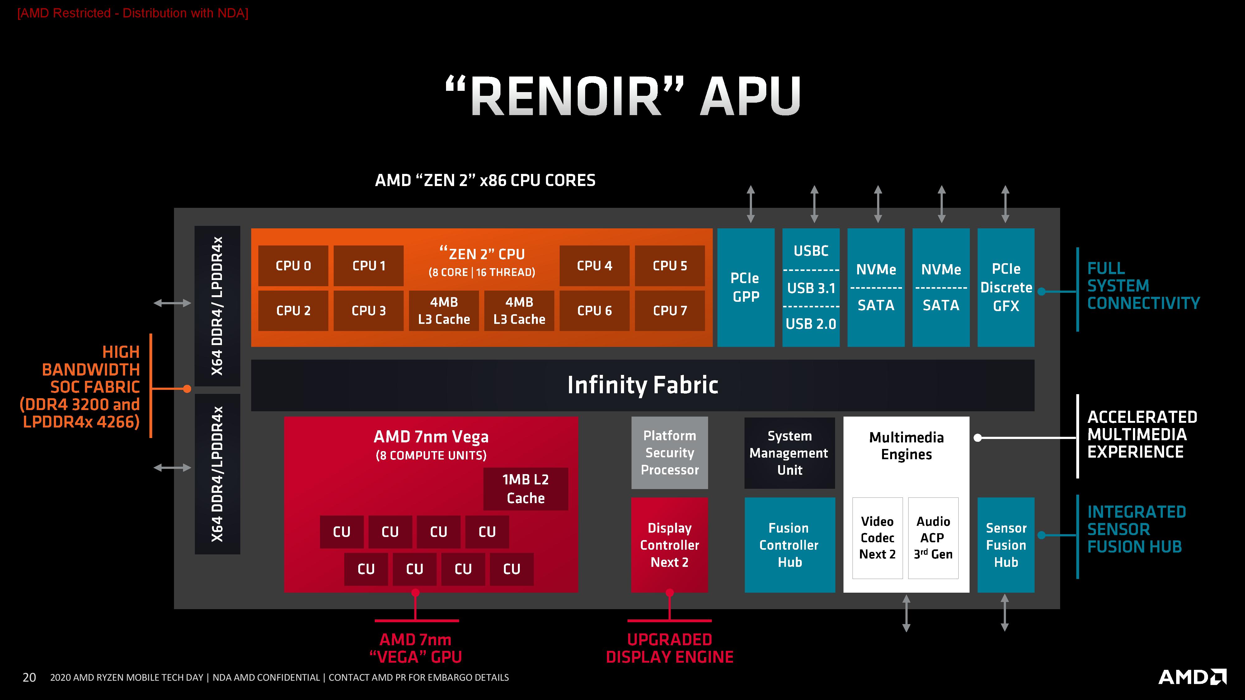
Also, AMD clearly updated the I/O block on Renoir significantly over Raven Ridge:
Wouldn't we all, but sadly that ain't happening any time soon. High resolution IR video is pretty much limited to the CIA and others with unlimited budgets. Even FLIR's highest-end imaging system intended for surveillance aircraft and the like tops out at 1280x720 IR sensors (with an option for 1080p upscaling). Their highest end professional handheld IR camera tops out at 1024x768 (starting at US$41 500).I want that IR video in high resolution. Watching the activity right on the silicon is mesmerizing.


