Speculation: Ryzen 4000 series/Zen 3

Page 130 - Seeking answers? Join the AnandTech community: where nearly half-a-million members share solutions and discuss the latest tech.

Valantar

Golden Member
Aug 26, 2014
1,792
508
136
@Valantar on your earlier post about Renoir PCIe resources...

Has the actual package pin-out for Mobile Renoir changed? I don't recall reading where it has new pins, and seeing that the 4000 series APUs are destined for desktop work shortly on AM4, it wouldn't seem like there has been any reconfiguration of the PCIe output (active pins) of the processor itself. At best, it looks, at least to me, like AMD has made some uefi and controller changes to the platform to allow the package pins that would normally go to the PCH/South-Bridge to instead drive a second m.2 slot on mobile configurations, leaving the rest of the PCIe output broadly the same, save for enabling unused lanes from Raven Ridge. Since the desktop AM4 socket isn't changing, it would seem that, at the most, they have made the needed PCIe controller changes internally to allow the output of a full x16 on the channel that drives the first (and/or second) full length PCIe slot on most motherboards. Of course, that does leave the question: does it support any native bifurcation on the socket driven x16?
They might have incorporated the necessary pins for x16 in the mobile package from the beginning and simply not populated them until now; the size and cost difference would be minimal. As for desktops, remember that desktop and mobile packages are completely separate pieces of hardware, and AMD can put whatever traces they want between whatever features are on the die and whatever pins are on the package as long as it fits the specification they have given to motherboard manufacturers and the like.

Also, AMD clearly updated the I/O block on Renoir significantly over Raven Ridge:
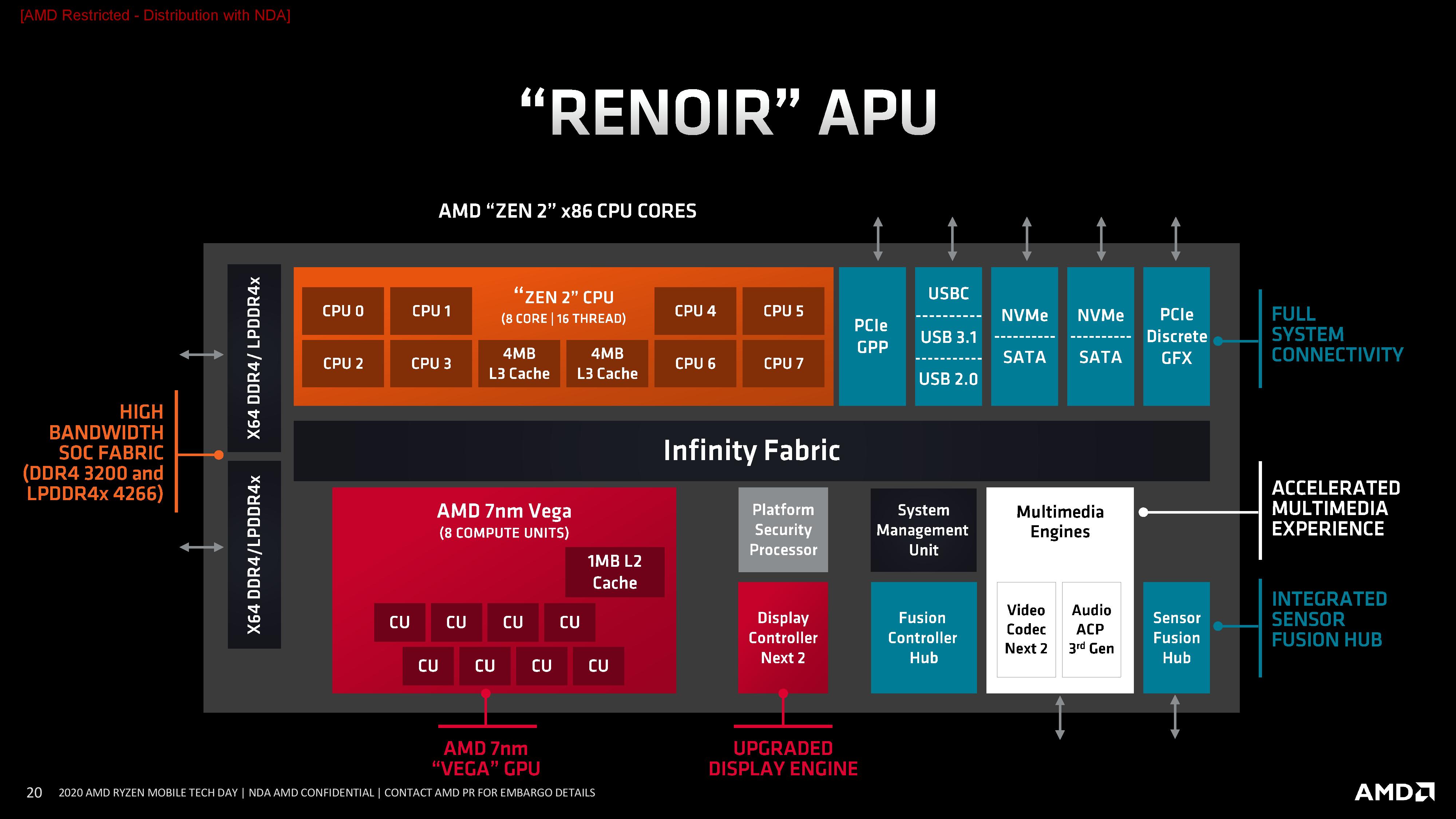
2%20AMD%20Ryzen%20Mobile%20Tech%20Day_General%20Session_Architecture%20Deep%20Dive-page-020.jpg
Also, saying "AMD has made some UEFI and controller changes" to increase PCIe lane count makes no sense but no change to the active pins makes no sense. Pins are active if they are connected to something and there is the possibility of transmitting a signal or power through them. Clearly the last x8 PCIe lanes on an x16 output connected to an x8 controller would thus not be active. For an increase in internal controller lanes to be usable outside of the die this obviously requires hooking these lanes up to pins, which again requires there to be free - thus activating previously disconnected pins. On Raven Ridge and previous APUs half of the lanes for the x16 slot weren't connected to anything at all. Now, these same lanes are fully populated with PCIe lanes. Thus, they were previously inactive, yet are now active. See?
I want that IR video in high resolution. Watching the activity right on the silicon is mesmerizing.
Wouldn't we all, but sadly that ain't happening any time soon. High resolution IR video is pretty much limited to the CIA and others with unlimited budgets. Even FLIR's highest-end imaging system intended for surveillance aircraft and the like tops out at 1280x720 IR sensors (with an option for 1080p upscaling). Their highest end professional handheld IR camera tops out at 1024x768 (starting at US$41 500).
 

LightningZ71

Golden Member
Mar 10, 2017
1,627
1,898
136
With the internal logic and UEFI changes, I meant that they had adapted the x4 link to the chipset, which is normally not used on mobile, to instead drive the second M.2 nvme slot at x4. From what little that I've seen of system reviews, the systems that have two M.2s are fully provisioning them with 4 lanes, and at least two of them also provide, from the processor, a data channel for an additional internal drive. That's too many lanes without either repurposing the x4 that was meant for the chipset or driving them from the top x8 from the x16 dGPU path.
 

amd6502

Senior member
Apr 21, 2017
971
360
136
AMD has been making the APU based on the previous generation; Ryzen 4000 APUs are Zen 2 based. I could see them wanting to change that, so perhaps they are working on getting a Zen 3 / RDNA2 APU out on 5 nm as early as possible. They would want both for better power efficiency.

I think 7nm+ is almost as good as 5nm, so it wouldn't be worth it until 5nm matures. I think there will be two APU projects on 7nm+. Big and small, and I think small could come out even before the Matisse successor. It would make quite a bit of sense for that to happen.
 

amd6502

Senior member
Apr 21, 2017
971
360
136
Do any of you think we'll see a new IO die? with a GPU?

I guess not for Zen2 since Renoir covers that, but for Zen3 perhaps?
 

HurleyBird

Platinum Member
Apr 22, 2003
2,682
1,266
136
Pretty sure Zen 3 will have a new IOD, if only because of the 8 core CCX. And judging by X570 power consumption, the Zen 2 IOD sort of sucks anyway.

What will be interesting is if they reuse the Zen 3 IOD for X670 or some other chipset (eg. ThreadRipper).
 

Valantar

Golden Member
Aug 26, 2014
1,792
508
136
With the internal logic and UEFI changes, I meant that they had adapted the x4 link to the chipset, which is normally not used on mobile, to instead drive the second M.2 nvme slot at x4. From what little that I've seen of system reviews, the systems that have two M.2s are fully provisioning them with 4 lanes, and at least two of them also provide, from the processor, a data channel for an additional internal drive. That's too many lanes without either repurposing the x4 that was meant for the chipset or driving them from the top x8 from the x16 dGPU path.
I got that, it's just that they still needed to add the lanes + connect the pins to make the x8 GPU connection into an x16. So there are changes to the pinout of Renoir desktop APUs compared to previous ones. As for NVMe, as you can see from the slide in my previous post, mobile APUs have two x4 links for m.2 drives, an x16 for GPUs, and some undefined number of general purpose lanes for WiFi and the like. If any laptop has the option for a third NVMe drive it's likely bifurcated off the x16 (seeing how no laptop GPUs tend to use x16 connections anyhow).
 

Valantar

Golden Member
Aug 26, 2014
1,792
508
136
Do any of you think we'll see a new IO die? with a GPU?

I guess not for Zen2 since Renoir covers that, but for Zen3 perhaps?
They're not going to put a GPU in the IOD, there's no point - a meaningful GPU would be too big to fit in the IOD (remember, I/O doesn't shrink well with node changes, so the IOD would be big even on 7nm), and there wouldn't be any point to adding a stripped-down one given that their customers have told them quite clearly that they don't need an iGPU for their CPUs.

It's much more likely we'll see an MCM APU at some point down the line, with one CCD, one IOD and one ... "GPD"? Though this would be problematic on mobile simply because of the added Z-height of an MCM package due to the more complex traces in the substrate.
Pretty sure Zen 3 will have a new IOD, if only because of the 8 core CCX. And judging by X570 power consumption, the Zen 2 IOD sort of sucks anyway.

What will be interesting is if they reuse the Zen 3 IOD for X670 or some other chipset (eg. ThreadRipper).
Why would the 8-core CCX necessitate a new IOD? The CCD will connect to the IOD over IF same as always, right? As for power consumption, I kind of doubt a single node change will make much of a difference. And, of course, I/O doesn't shrink well. It's PCIe 4.0 by itself that needs that kind of power; the signalling is far more complex, and it's handing 2x the data compared to 3.0 after all, so power consumption will always be higher.
 

VirtualLarry

No Lifer
Aug 25, 2001
56,324
10,034
126
Pretty sure Zen 3 will have a new IOD, if only because of the 8 core CCX. And judging by X570 power consumption, the Zen 2 IOD sort of sucks anyway.

What will be interesting is if they reuse the Zen 3 IOD for X670 or some other chipset (eg. ThreadRipper).
IF they add a (small, desktop-functional) iGPU to the "new IOD"... what if they introduce that as a new system chipset, X670, and have an actual "chipset iGPU" again? Or they could put it on the CPU die. But honestly, it wouldn't be a horrible thing, would it, for the system chipset to contain the iGPU again? Unless, that could cause interference (requiring a switch) between an actual APU's video output pins, and the chipset iGPU's output pins. That might complicate things somewhat.

Or maybe they should bifurcate the system chipsets, and make ones FOR APUs, that would pass-through the video outputs, and make ones FOR CPUs, with a (small) chipset iGPU, primarily designed for "business desktops", with Ryzen CPUs. Kind of like Intel's Q-series chipsets. Obscure, OEM-only, but designed specifically for business desktops. Maybe bundle those (with chipset iGPUs) with Ryzen PRO CPUs.

Edit: Not entirely unlike the 760G, 780G, and 970, 990X, and 990FX chipsets that AMD had for AM3/AM3+.
 

Valantar

Golden Member
Aug 26, 2014
1,792
508
136
IF they add a (small, desktop-functional) iGPU to the "new IOD"... what if they introduce that as a new system chipset, X670, and have an actual "chipset iGPU" again? Or they could put it on the CPU die. But honestly, it wouldn't be a horrible thing, would it, for the system chipset to contain the iGPU again? Unless, that could cause interference (requiring a switch) between an actual APU's video output pins, and the chipset iGPU's output pins. That might complicate things somewhat.

Or maybe they should bifurcate the system chipsets, and make ones FOR APUs, that would pass-through the video outputs, and make ones FOR CPUs, with a (small) chipset iGPU, primarily designed for "business desktops", with Ryzen CPUs. Kind of like Intel's Q-series chipsets. Obscure, OEM-only, but designed specifically for business desktops. Maybe bundle those (with chipset iGPUs) with Ryzen PRO CPUs.

Edit: Not entirely unlike the 760G, 780G, and 970, 990X, and 990FX chipsets that AMD had for AM3/AM3+.
Bespoke CPU/APU chipsets is a terrible idea, it would utterly decimate the selection of motherboards available for APUs. It would for all intents and purposes kill DIY apu sales, relegating them to pre-builts alone. Plus it would removeany upgrade path for APU buyers. Two platforms (HEDT + MSDT) is more than enough.

Besides that, a chipset iGPU with the option for an APU would require some sort of mux for every video output, so up to three per board, plus the traces for getting those signals from the chipset to the output - which is generally on the opposite side of the board from where the chipset sits. Sounds like a noticeable cost increase for relatively little value IMO.
 

french toast

Senior member
Feb 22, 2017
988
825
136
What is the chances when AMD does move to a new IOD die (Zen 4 I think), that they tap up Samsung 8nm for that?
Probably get a good deal, lots of capacity without affecting Tsmc supply, mature optimised process so performance and yields will be terrific.

What kind of performance benefits would that enable vs Global foundries 12nm?
 

maddie

Diamond Member
Jul 18, 2010
4,738
4,667
136
What is the chances when AMD does move to a new IOD die (Zen 4 I think), that they tap up Samsung 8nm for that?
Probably get a good deal, lots of capacity without affecting Tsmc supply, mature optimised process so performance and yields will be terrific.

What kind of performance benefits would that enable vs Global foundries 12nm?
Another possibility.

GlobalFoundries Unveils 12LP+ Technology: Massive Performance & Power Improvements
https://www.anandtech.com/show/1490...nology-massive-performance-power-improvements

'GlobalFoundries’ 12LP+ manufacturing technology builds upon the company’s 12LP process yet enables a 20% increase in performance (at the same power and complexity) or a 40% reduction in power requirements (at the same clocks and complexity) as well as a 15% improvement in logic area scaling when compared to 12LP platform'
..........................
'GlobalFoundries expects its customers to tape out the first 12LP+ SoCs sometimes in the second half of 2020 and produce them in volume in 2021.'
 

Valantar

Golden Member
Aug 26, 2014
1,792
508
136
Another possibility.

GlobalFoundries Unveils 12LP+ Technology: Massive Performance & Power Improvements
https://www.anandtech.com/show/1490...nology-massive-performance-power-improvements

'GlobalFoundries’ 12LP+ manufacturing technology builds upon the company’s 12LP process yet enables a 20% increase in performance (at the same power and complexity) or a 40% reduction in power requirements (at the same clocks and complexity) as well as a 15% improvement in logic area scaling when compared to 12LP platform'
..........................
'GlobalFoundries expects its customers to tape out the first 12LP+ SoCs sometimes in the second half of 2020 and produce them in volume in 2021.'
Power numbers like those are typically for logic, not I/O, so power scaling for an I/O die is likely to be significantly worse than that. Same for area, and performance doesn't matter much for that application.
 

moinmoin

Diamond Member
Jun 1, 2017
4,944
7,656
136
While I do expect the concept of an IOD to stay for Zen 3 (there I expect the big changes to happen within the cores), in line with keeping AM4 compatibility, for Zen 4 I'm kind of anticipating another radical platform design switch like happened between Zen 1 and 2. At that point the moniker "IOD" may well be no longer applicable.
 

LightningZ71

Golden Member
Mar 10, 2017
1,627
1,898
136
I got that, it's just that they still needed to add the lanes + connect the pins to make the x8 GPU connection into an x16. So there are changes to the pinout of Renoir desktop APUs compared to previous ones. As for NVMe, as you can see from the slide in my previous post, mobile APUs have two x4 links for m.2 drives, an x16 for GPUs, and some undefined number of general purpose lanes for WiFi and the like. If any laptop has the option for a third NVMe drive it's likely bifurcated off the x16 (seeing how no laptop GPUs tend to use x16 connections anyhow).

I'm sorry that I wasn't more specific. The third drive that I was referencing was SATA, not NVME. We know that previous Zen processors made you choose with respect to the drive I/O coming out of the processor: one x4 NVME, or one x2 NVME and a pair of SATA ports. Now, we have Renoir, which looks like it has the ability to drive a pair of x4 NVME devices and also can drive at least one SATA lane, all without using an external controller. Either the Renoir die has a massive tear up and redo of the PCIe side of things inside the package, or, they've repurposed the x4 chipset link to drive one NVME slot (not a big deal, they are both essentially just PCIe devices) and also bifurcating the x16 PCIe link down to x8/x4(and x4 unused unless that's what's driving the wireless cards) to drive both the dGPU and an M.2 NVME. The sata drive is being driven by the existing provision for the x4 NVME link to be split to x2+2 sata.

I'm not complaining about any of this, just wrapping my head around it all.
 
  • Like
Reactions: Valantar

LightningZ71

Golden Member
Mar 10, 2017
1,627
1,898
136
Part of the problem with scaling the I/O die is pin out, specifically, getting the signals in and out of the die itself. That requires a lot of "macro-scale" contact points that have to be separated from each other. The logic behind driving all of those interfaces shrinks just about as well as the rest of the logic in the processors, with the exception of what are effectively capacitors that help stabilize the connections themselves. With improvements in shrinking the pin outs (going to a finer grid pitch/ smaller spacing between "pins"), the logic can be further shrunk on the I/O die with new processes. However, it's absolutely going to scale more slowly than normal logic, which is why it is a boon to AMD to have chosen to use a separate I/O die in the same package.
 

Valantar

Golden Member
Aug 26, 2014
1,792
508
136
I'm sorry that I wasn't more specific. The third drive that I was referencing was SATA, not NVME. We know that previous Zen processors made you choose with respect to the drive I/O coming out of the processor: one x4 NVME, or one x2 NVME and a pair of SATA ports. Now, we have Renoir, which looks like it has the ability to drive a pair of x4 NVME devices and also can drive at least one SATA lane, all without using an external controller. Either the Renoir die has a massive tear up and redo of the PCIe side of things inside the package, or, they've repurposed the x4 chipset link to drive one NVME slot (not a big deal, they are both essentially just PCIe devices) and also bifurcating the x16 PCIe link down to x8/x4(and x4 unused unless that's what's driving the wireless cards) to drive both the dGPU and an M.2 NVME. The sata drive is being driven by the existing provision for the x4 NVME link to be split to x2+2 sata.

I'm not complaining about any of this, just wrapping my head around it all.
According to AMD themselves, mobile Renoir has two storage blocks, each of which can be either an x4 NVMe drive or some unknown SATA configuration. It might be possible for one of them to be x2 NVMe and SATA I suppose, but at least according to AMD's own block diagram of mobile Renoir, that's all the storage I/O it has. Of course in a dGPU-less system it would be entirely possible to populate at least x4 of the PEG PCIe lanes with another NVMe slot, leaving one of the storage blocks free to be used as SATA. It might also be possible to do this with a dGPU, though that depends if the x16 controller supports bifurcation or not. See my previous post for the diagram, sourced from AT's launch coverage.

While I do expect the concept of an IOD to stay for Zen 3 (there I expect the big changes to happen within the cores), in line with keeping AM4 compatibility, for Zen 4 I'm kind of anticipating another radical platform design switch like happened between Zen 1 and 2. At that point the moniker "IOD" may well be no longer applicable.
Are you thinking they will further split up the I/O? I sincerely doubt they'll go back to a monolithic design given the massive success of their MCM designs.
 

french toast

Senior member
Feb 22, 2017
988
825
136
Well, it would be smaller. Take up less package space. Probably.
Along with optimisations and experience gained Regards to building IOD die, I would hope so, would this enable higher higher fabric clocks = lower latency?
Another possibility.

GlobalFoundries Unveils 12LP+ Technology: Massive Performance & Power Improvements
https://www.anandtech.com/show/1490...nology-massive-performance-power-improvements

'GlobalFoundries’ 12LP+ manufacturing technology builds upon the company’s 12LP process yet enables a 20% increase in performance (at the same power and complexity) or a 40% reduction in power requirements (at the same clocks and complexity) as well as a 15% improvement in logic area scaling when compared to 12LP platform'
..........................
'GlobalFoundries expects its customers to tape out the first 12LP+ SoCs sometimes in the second half of 2020 and produce them in volume in 2021.'
Interesting, why would global foundries develop such a process without a know significant customer? If this rings true then this is very impressive imo.
I now think this is the favourite scenario for Zen 4 IOD, far too convenient imo.
I think zen 3 IOD will stay the same.
Power numbers like those are typically for logic, not I/O, so power scaling for an I/O die is likely to be significantly worse than that. Same for area, and performance doesn't matter much for that application.
True, but maybe this process was specifically designed for this use case, it must improve the performance, even if just allows increased fabric speeds relative to mem clock to reduce latency or something? Allow ddr5 at effective speeds and decent efficiency.
PCIE 5?.. Possible small gpu for OEM office market? They are going to need every bit of help they can with process.
 

moinmoin

Diamond Member
Jun 1, 2017
4,944
7,656
136
Are you thinking they will further split up the I/O?
This indeed. @LightningZ71 mentioned it already, pin-out is a potential problem for shrinking the IOD. So the uncore logic could be split up between an interposer which ideally houses all the connections such as all the PHYs and IFOPs endpoints etc. whereas some stapled dies could house the secret sauce (unfortunately we know way too little about Zen's uncore, but I'd expect that to include things like the PSP, fabric switches, buffers, SerDes and memory controller, I/O root hub and tag directories etc.).

In general I can imagine AMD keeping using MCM for some parts even after introducing interposer and X3D chip stacking, as MCM has its advantage in allowing longer paths between separate dies.
 
  • Like
Reactions: amd6502

VirtualLarry

No Lifer
Aug 25, 2001
56,324
10,034
126
I thought that people said that the Zen SoC had 32 PCI-E lanes coming off it (die), whereas, the AM4 package only had 24 PCI-E lanes coming off of the
CPU (16x for GPU, 4x for NVMe, 4x for chipset, and some SATA lanes).
 

HurleyBird

Platinum Member
Apr 22, 2003
2,682
1,266
136
It was confirmed (again) by AMD today that they will have Zen 3 in 2020, and that it will be 7nm, not 5nm as was being tossed around at times.
TechPowerUp

Technically, today AMD only said the former. They didn't mention 5 or 7nm, although TPU takes as confirmation the recent slide references 7nm for Zen 3. Theoretically, if AMD has both 5nm and 7nm versions of the Zen 3 chiplet cooking, then referencing 7nm isn't lying about 5nm even if it's a bit sneaky.

What's more damning in my eyes for the 5nm speculation is that both rumours came from Digitimes, and now the general veracity of their Zen 3 information in serious doubt.