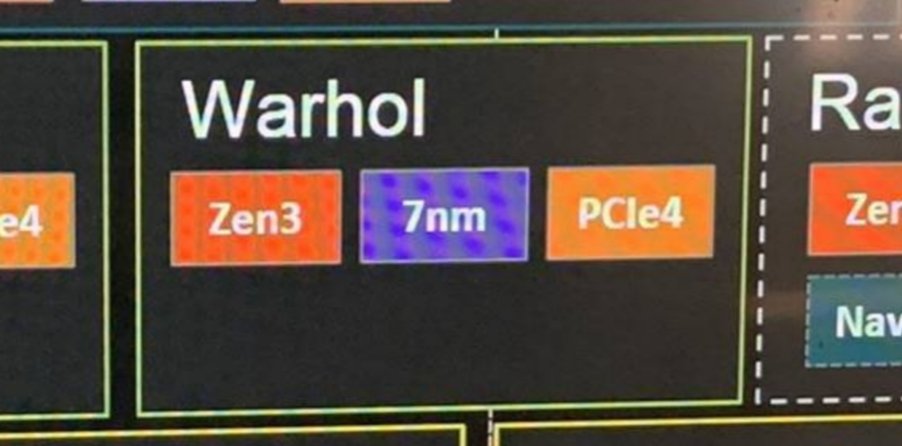
Speculation: Ryzen 4000 series/Zen 3

Page 124 - Seeking answers? Join the AnandTech community: where nearly half-a-million members share solutions and discuss the latest tech.

RetroZombie

Senior member
Nov 5, 2019
464
386
96
I can't even keep up with the leaks...
They might have put some IA police to work releasing random code names on random tsmc processes to catch out leakers so watch out. :p


On a serious note what i always expected for zen4 was just zen3 shrink into 5nm with two eight core ccx instead of one in the zen3, so zen4 design would be immediately released has soon as the 'new' process would be available.

There's also the frontier cpu for the DOE:
AMD Confirms Zen 4 EPYC Codename, and Elaborates on Frontier Supercomputer CPU
Forrest explained that the CPU is not Milan – it is actually a fully custom design CPU specifically for this project.
 
Last edited:

maddie

Diamond Member
Jul 18, 2010
4,744
4,679
136
That's where I stand as well. No way AMD is moving an N7+ design to N5P (which don't use the same design rules) on such a short notice, with the former already being used for sampling in datacenters. TSMC is accelerating mass production N5P, so may have asked AMD to do the same for its silicon design already in the work for N5P which would be Zen 4, not 3. Though AMD's first N5P design actually realistically would be a GPU pipecleaner. This report doesn't amount to much imo.
I really can't see Zen4 being able to be pulled in so quickly, whereas migrating Zen3 from 7EUV to 5Euv should be a lot easier and quicker. As I posted earlier, there's no rule preventing Zen3 on both 7nm and 5nm. One for server (7nm) and the other for desktop (5nm). I know everyone thinks that it must be the other way, but I see a good reason for it this way. The I/O die design is common to all in any case. Isn't this one of the benefits of a chiplet design. Should AMD religiously follow the stated roadmap, even in the face of quicker advancement?

Anyone can estimate the time needed to migrate a synthesizable design to a different node using the same RTL file? Isn't this exactly what AMD has worked so hard to exploit in order to be agile?
 

DisEnchantment

Golden Member
Mar 3, 2017
1,608
5,810
136
Anyone can estimate the time needed to migrate a synthesizable design to a different node using the same RTL file? Isn't this exactly what AMD has worked so hard to exploit in order to be agile?
From RTL is still too high level. So many steps still involved.
Physical design, layout, place and route, signal integrity, clock domains, power planes etc behave differently on different processes due to difference of the electrical characteristics of the different layers. High frequency designs are even more affected by these.
~8-10 months is being extremely optimistic.
That said you can buy ready made libraries from Synopsys or someone for that particular process and speed up things. But there are things which are your own stuffs like cores, power design and stuff which you need to redo.
 

maddie

Diamond Member
Jul 18, 2010
4,744
4,679
136
From RTL is still too high level. So many steps still involved.
Physical design, layout, place and route, signal integrity, clock domains, power planes etc behave differently on different processes due to difference of the electrical characteristics of the different layers. High frequency designs are even more affected by these.
~8-10 months is being extremely optimistic.
That said you can buy ready made libraries from Synopsys or someone for that particular process and speed up things. But there are things which are your own stuffs like cores, power design and stuff which you need to redo.
Taking 12 months as possible with some dedicated work, would mean that they needed to start last Dec or Jan for a late 2020 release. The whole extreme secrecy about Zen3 tells me something is afoot. 3-5 months before a possible release and no leaks. Surely MB manufacturers would have had access to early models already. True?
 

moinmoin

Diamond Member
Jun 1, 2017
4,952
7,666
136
Taking 12 months as possible with some dedicated work, would mean that they needed to start last Dec or Jan for a late 2020 release. The whole extreme secrecy about Zen3 tells me something is afoot. 3-5 months before a possible release and no leaks. Surely MB manufacturers would have had access to early models already. True?
The port would need to be finished before a tape out. And tape outs usually happen a little less than a year before volume production. Samples are created from that point on.
 
  • Like
Reactions: lightmanek

DisEnchantment

Golden Member
Mar 3, 2017
1,608
5,810
136
Taking 12 months as possible with some dedicated work, would mean that they needed to start last Dec or Jan for a late 2020 release. The whole extreme secrecy about Zen3 tells me something is afoot. 3-5 months before a possible release and no leaks. Surely MB manufacturers would have had access to early models already. True?
They need to have started migrating to the N5 PDK beforehand. PDK is available even before process is ready. From there they do tape out. After tapeout they optimize the physical design, layout, routing and such. TSMC provides cloud based infrastructure to simulate this and they are doing a lot to speed this up so that porting designs to new PDK is faster.

ARM SoCs are typically faster in migrating.
But high frequency x86 are more challenging because of signal integrity, clocks, propagation delays, races and so on
I read somewhere it is faster to migrate GPUs to new nodes.

Also verification of x86 chips is a lot complex.
 

LightningZ71

Golden Member
Mar 10, 2017
1,628
1,898
136
TSMC N5 isn't exactly brand spanking new. Apple has been producing volume on it for a while now. N5P is supposedly just a refinement of it, and was planned for over a year ago. So, this isn't some mystery node that just appeared out of thin air.

I contend that AMD has learned it's lesson from past troubles with being beholden to a single upcoming foundary node and, now that they actually have a decent revenue stream, have been hedging their bets by designing for multiple target nodes. We also know that TSMC has been helping their customers with this process to increase their foundary utilization numbers and to get quicker ROI as well as to guard against customers leaving for Samsung. It is not impossible that AMD and TSMC have worked together to get ZEN 3 ready on both N7(improved) and N5P.
 

uzzi38

Platinum Member
Oct 16, 2019
2,635
5,979
146
I can't even keep up with the leaks...

AMD Ryzen 5000 Zen3 “Warhol” to succeed Vermeer

This one is BS.

The poster of that rumour is trying to push that Zen 4 and AMD using 5nm for the first time is Q2-Q3 2022, which is completely and utterly wrong. Ignore anything he says.
 

moinmoin

Diamond Member
Jun 1, 2017
4,952
7,666
136
TSMC N5 isn't exactly brand spanking new.
April 2020 volume production is very sparkly though.

It is not impossible that AMD and TSMC have worked together to get ZEN 3 ready on both N7(improved) and N5P.
True, I thought the details of AMD adaption to N7 showed they should have a close working relationship indeed.

Though it warrants to remember that the whole process in getting chips to be created on those finer nodes is the most expensive part of producing chips nowadays. So with AMD's greediness wrt the number of different die designs I find it hard to believe they pay for the whole upfront process cost without any intention to making use of it. That's why I don't think they'd have the same design on incompatible different nodes.
 

Ajay

Lifer
Jan 8, 2001
15,458
7,862
136
They need to have started migrating to the N5 PDK beforehand. PDK is available even before process is ready. From there they do tape out. After tapeout they optimize the physical design, layout, routing and such. TSMC provides cloud based infrastructure to simulate this and they are doing a lot to speed this up so that porting designs to new PDK is faster.
Tapeout, IIRC, is for creating the masks and, I assume, process steps (etch, poly, metal, etc.).
 

JasonLD

Senior member
Aug 22, 2017
485
445
136
Zen 3 is already expected to be decent improvement over Zen 2 on improved N7. I don't see why AMD has to alter that plan and accelerate to 5nm while sacrificing margin and yield they would get from 7nm. It would make sense if Intel pulls a surprise move to 7nm next year but chance of that happening is close to zero.
 

maddie

Diamond Member
Jul 18, 2010
4,744
4,679
136
Zen 3 is already expected to be decent improvement over Zen 2 on improved N7. I don't see why AMD has to alter that plan and accelerate to 5nm while sacrificing margin and yield they would get from 7nm. It would make sense if Intel pulls a surprise move to 7nm next year but chance of that happening is close to zero.
There is a battle for leading edge wafers ongoing. Why is this ignored. Does anyone think AMD or any other company could just decide arbitrarily on when they alone need a certain product and not account for others snapping up future production? Use it or lose it appears to be the game with TSMC at present as they are the clear fab leader. This has to be factored in whatever changes might have been made to roadmaps.
 

JasonLD

Senior member
Aug 22, 2017
485
445
136
There is a battle for leading edge wafers ongoing. Why is this ignored. Does anyone think AMD or any other company could just decide arbitrarily on when they alone need a certain product and not account for others snapping up future production? Use it or lose it appears to be the game with TSMC at present as they are the clear fab leader. This has to be factored in whatever changes might have been made to roadmaps.

At what cost? It doesn't make a business sense to alter what is already a solid roadmap just to get on board with leading edge node asap while giving up on proven node with great yield, margin, and volume.
 
  • Like
Reactions: yuri69 and teejee

maddie

Diamond Member
Jul 18, 2010
4,744
4,679
136
At what cost? It doesn't make a business sense to alter what is already a solid roadmap just to get on board with leading edge node asap while giving up on proven node with great yield, margin, and volume.
Not to get on board ASAP by itself, but if you don't get on board when offered you might have to wait longer than expected for when production scales up. Others will have taken your position. Do you expect TSMC to keep production capacity idle while AMD or anybody decides when is the right time to advance? They sell capacity as soon as possible and it's up to their customers to reserve volume. As I said, use it or lose it.

TSMC right now can be seen as kingmakers.
 

itsmydamnation

Platinum Member
Feb 6, 2011
2,773
3,151
136
The thing to remember is amd x86 doesn't complete with any other TSMC customers for end sales. So from a revenue growth from TSMC perspective, getting amd to buy big wafers on new process is massive growth. TSMC can always build more fabs.

Now the questions are, how early did TSMC think 5nm was a homerun / working great. How early/did AMD/TMSC talk about accelerating to 5nm. What products does that line up to.
 

lightmanek

Senior member
Feb 19, 2017
387
754
136
The thing to remember is amd x86 doesn't complete with any other TSMC customers for end sales. So from a revenue growth from TSMC perspective, getting amd to buy big wafers on new process is massive growth. TSMC can always build more fabs.

Now the questions are, how early did TSMC think 5nm was a homerun / working great. How early/did AMD/TMSC talk about accelerating to 5nm. What products does that line up to.

I remember our NostaSeronox telling everyone that TSMC gave AMD an offer to accelerate 5nm adoption or be left behind a long time ago. I vaguely remember it was around Zen2 launch, so this would give enough time to realign some of the plans.
When I'm not on the phone, I might try to find that post, or maybe poster himself can tune in and refresh our memories.
 
  • Wow
Reactions: spursindonesia

NTMBK

Lifer
Nov 14, 2011
10,239
5,025
136
I remember our NostaSeronox telling everyone that TSMC gave AMD an offer to accelerate 5nm adoption or be left behind a long time ago. I vaguely remember it was around Zen2 launch, so this would give enough time to realign some of the plans.
When I'm not on the phone, I might try to find that post, or maybe poster himself can tune in and refresh our memories.

Holy crap, you're right!

Hot and spicy rumor, get out your table salt.

AMD has canned all 7nm+(7nm EUV) projects that are APU/CPU/GPU 2.5D/3D. AMD instead will be launching them on the 5nm node at the soonest.

7nm DUV, 7nmP DUV, 5nm EUV is the new timeline from an unnamed individual from TW.

Stuff to watch out for: RRD. Three new CCDs at TSMC. Of which one is for the new Renoir(7nm) and its successor Rembrandt(5nm). The D one is for a semi-custom project on 6nm(not AMD mainline, however it might get pushed to 5nm).

TSMC doesn't like the 7nm/7nm+ as first customer, so they want AMD to be on 5nm.


Valantar

Golden Member
Aug 26, 2014
1,792
508
136
Holy crap, you're right!


Interesting, though there's a rather glaring factual error there: calling Renoir a CCD. Monolithic dice are not CCDs, so something there doesn't add up. Of course that might just mean that the entire "RRD" thing is monolithic chips and not CCDs.
 

jpiniero

Lifer
Oct 1, 2010
14,605
5,224
136
There's also the frontier cpu for the DOE:
AMD Confirms Zen 4 EPYC Codename, and Elaborates on Frontier Supercomputer CPU
Forrest explained that the CPU is not Milan – it is actually a fully custom design CPU specifically for this project.

I was going to say that if they were going to release anything 5 nm that soon, it would be HPC related. I suppose it could include a CPU too that could be repurposed for desktops at some point. The timing doesn't match up for me for for it to directly replace releasing Vermeer though.
 

uzzi38

Platinum Member
Oct 16, 2019
2,635
5,979
146
Holy crap, you're right!
Yeah, this rumour is one of the things that makes me think that N5P is actually for Rembrandt first, not for Vermeer/Milan. The guy's LinkedIn profile did pretty clearly say he was working with 5/6/7nm and had worked on Renoir/Durango/Rembrandt in no particular order.

However, there is one more rumour to discuss regarding all of this.
The poster here is apparently saying there wasn't a retape to N5P but instead to N6. It's uh, still extremely unlikely to say the least... but this guy did leak the RDNA2 die sizes, and the size for Navi21 that he talked about I am pretty confident is accurate at least, so it's hard to ignore what he's written.
 

jpiniero

Lifer
Oct 1, 2010
14,605
5,224
136
I thought Vermeer was intended to be 7+... 6 wouldn't make sense. The timing would be correct I think, Q1 21 is when 6 is supposed to be first available.
 
  • Like
Reactions: Tlh97 and uzzi38

uzzi38

Platinum Member
Oct 16, 2019
2,635
5,979
146
I thought Vermeer was intended to be 7+... 6 wouldn't make sense.
You're right, it doesn't. I agree actually. N7+ isn't IP compatible with N6... N7P is though. I did post the rumour, but by no means did I think what he said about Vermeer/Milan was likely.

I wouldn't be surprised if he's right about Navi23, but I can't see it happening for Zen 3 based products.
 

NostaSeronx

Diamond Member
Sep 18, 2011
3,686
1,221
136
N6 wasn't IP-compatible in 2019, but it should eventually be IP-compatible. TSMC 7nm DUV can move to 6nm EUV(Cx=Mx) and 7nm EUV can move to 6nm EUV(2/3Cx=Mx). Everything is planned to be pushed towards 6nm as the long-term node. As it upports some of the EUV tweaks from 5nm for the 7nm nodes.

AMD's 7nm at TSMC isn't a custom-grade node(like: GF28SHP/GF28A/GFFinFET-Boost+) but the 5nm that AMD will be using is a custom-grade node. So, while 7nm AMD is exactly 1:1 with the TSMC perf/power, 5nm TSMC with AMD might have more performance/power than published by TSMC for N5.

Altered LG/MG/SG/EG stuff => 0.5V->0.6V/0.75V->0.85V/1V->1.1V/1.2V->1.25V/1.5V->1.55V/1.8V->2.1V etc
Increased SiGe/Spacer/Vt tweaks per year(N5A -> N5A+ -> N5A++, A standing for AMD) => 2020(baseline) -> 2021(5% improvement) -> 2022(7.5% improvement), etc
(Hisilicon is supposedly in an agreement to re-use AMD's tweaks, with them making custom-level standard cells for AMD)
 
Last edited:

LightningZ71

Golden Member
Mar 10, 2017
1,628
1,898
136
Well, Nosta's prognostications and leaks do relatively match up, though with the expected minor wording quibbles such leaks bring. We know that AMD has announced that Zen3 wasn't going on N7P, and was even cagey about it being on N7+, just noting that it was an "improved 7nm node". Renoir was too far along on N7 to change anything. This rumor of Zen3 being also on 5nm matches with TSMC desiring AMD to be on N5/N5P. IT also follows that at least some Zen3 CCDs will be made on improved N7 as the next EPYC parts have been in validation for some time. So, it shakes out like this:

Zen3: impN7 CCDs for Epyc and low end Ryzen. N5P CCDs for High end Ryzen and maybe Threadripper. A pair of APUs, one with VEGA and one with RDNA.
Zen4: It's reasonable to suspect that it will be on an improved N5P process unless N3 is drastically quicker than expected.
 
  • Like
Reactions: Tlh97