Errr... aren't they all linked through the L3 cache?I saw the slides. It doesn't show how the cores on each side of the massive L3 are linked at all. It shows four cores on the left and four on the right, with the L3 in between. And . . . that's it! No link diagram, no topology, no nothing. It does make it very clear that the cores are separated into two blocks just like in Rome. Just the L3 is different.

Speculation: Ryzen 4000 series/Zen 3
Page 38 - Seeking answers? Join the AnandTech community: where nearly half-a-million members share solutions and discuss the latest tech.
You are using an out of date browser. It may not display this or other websites correctly.
You should upgrade or use an alternative browser.
You should upgrade or use an alternative browser.
DrMrLordX
Lifer
- Apr 27, 2000
- 23,125
- 13,224
- 136
Errr... aren't they all linked through the L3 cache?
Who knows? They don't tell you. Look at the slide. See the similarities between Rome and Milan in the diagram?
It's possible that AMD plans on using L3 here as a sort-of "directory" to facilitate intercore communications across CCXs on the same CCD via cache synchronization (sort of like HT Assist from the old Opteron days). I think L3 latency is overall lower than inter-CCX latency on Zen2/Rome so that would make sense. For example, with an IF clock of 1866 MHz, my Matisse is showing ~65ns latency between CCXs on the same CCD (according to SiSoft Sandra). That's nearly identical to my DDR4-3733 14-16-14-28 mem latency (according to AIDA64; Sandra says my mem latency is 29.7ns but I know that's probably not true). In contrast, Sandra says that my L3 latency is ~20ns which is decidedly quicker. That being said, intra-CCX communications happen at 15-16ns so using L3 synchronization still won't be optimal compared to a "true" 8c CCX. It would be close, though, and it wouldn't require a more-complicated core topography compared to Zen2.
Last edited:
The similarities are quite intentional I believe, the term 'cock tease' comes to mind.Who knows? They don't tell you. Look at the slide. See the similarities between Rome and Milan in the diagram?
This is basically a teaser for a proper reveal later, and possibly also to dispell the SMT4 rumour as they specifically state it to be SMT2, in any other situation I would think that to be extraneous information to be assumed in its absence.
DrMrLordX
Lifer
- Apr 27, 2000
- 23,125
- 13,224
- 136
It does pose an interesting question of CCD bandwidth vs Zen2 though if the unification of the L3 cache means only one IF link to the IOD.
Perhaps we can infer an increase in IF link bandwitdh for Zen3 as there was from Zen1 to Zen2.
I expect more IF bandwidth regardless, either through higher IF speeds and/or wider links. But I'm reasonably confident that we'll see two IF links to the IOD per CCD just as with Zen2.
What's the difference between the 2?either through higher IF speeds and/or wider links.
Is the bandwidth of IF independent from the clock?
DrMrLordX
Lifer
- Apr 27, 2000
- 23,125
- 13,224
- 136
What's the difference between the 2?
Is the bandwidth of IF independent from the clock?
Actual IF bandwidth is going to be a product of: data transmitted per clock and clockspeed. So they can maintain the current default clocks of Rome, widen the link by 2x, and get twice the IF bandwidth. Or they can increase clocks by maybe 50% and get 50% more bandwidth and lower latency for communications that aren't already saturating the existing link. There are tradeoffs to either method wrt power and area.
uzzi38
Platinum Member
- Oct 16, 2019
- 2,746
- 6,655
- 146
Errr... aren't they all linked through the L3 cache?
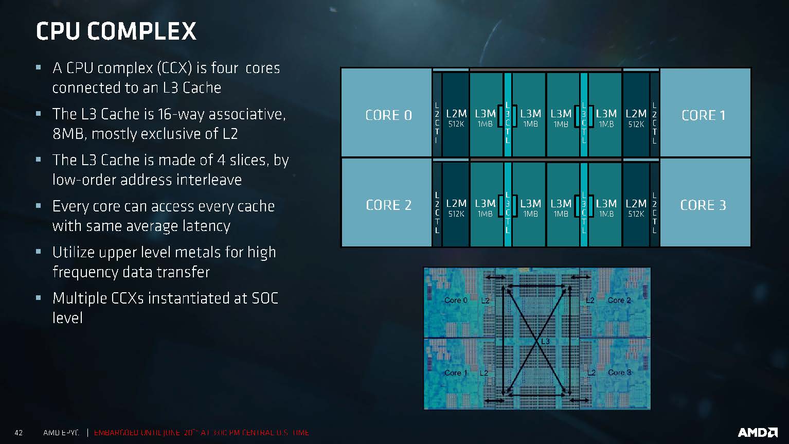
AFAIK they are, yes.
DisEnchantment
Golden Member
- Mar 3, 2017
- 1,779
- 6,797
- 136
Richie Rich
Senior member
- Jul 28, 2019
- 470
- 230
- 76
Most of those haters are from Eastern Europe/Russia area according to posting times. What do you expect from that area? In those countries they are not able to develop CPU but they are very good in naming hundreds of reasons why something is not possible. Even when Apple proved that 6xALU core is possible. It's funny and sad at the same time.Why all the intense hate for Richie Rich posts?
All he's saying is that 6 ALU will be faster than 4 ALU IF the rest of the support structures ( cache, decode, retire, etc) are in place. Not that 6 is always better than 4 irrespective of anything else.
itsmydamnation
Diamond Member
- Feb 6, 2011
- 3,096
- 3,941
- 136
Most of those haters are from Eastern Europe/Russia area according to posting times. What do you expect from that area? In those countries they are not able to develop CPU but they are very good in naming hundreds of reasons why something is not possible. Even when Apple proved that 6xALU core is possible. It's funny and sad at the same time.
Still waiting for your actual evidence of how 4xALU's being a bottleneck in SPEC, the only sad thing here is your lack of integrity by making big statements and then completely failing to back any of it up.
Still waiting to hear how you propose to feed these 6 ALU's with a 6 uop /4-5 x86 instructions issue limit and you have to do loads and stores within that.
Also no one said it was impossible, whats being question is the actual gain by doing so in a vacuum.
if AMD went 6x ALU's it wouldn't be the "killer feature"the killer features would be all the stuff that allowed you utilisation all those ALU's enough that the cost of them and the read/write ports to the PRF would be worth it. Execution of Data is easy, Movement of data is extremely hard. The fundamental difference between things like CPU's/GPU's/FPGA's/DSP etc is not execution its data movement.
overall you just need to get a clue..... Dunning Kruger and all that.
uzzi38
Platinum Member
- Oct 16, 2019
- 2,746
- 6,655
- 146
Welcome to AT. You have been very active on /r/Amd")
Thanks I guess :S
Though I've been more active on r/hardware recently.
I live in the UK and I often post at all times of the day or night, what time people post is meaningless.Most of those haters are from Eastern Europe/Russia area according to posting times.
H T C
Senior member
- Nov 7, 2018
- 610
- 451
- 136
I live in the UK and I often post at all times of the day or night, what time people post is meaningless.
Blizzard banned me from Diablo III accusing me of using "automated programs" because i played @ all hours. When one works in rotating shifts, one tends to be unable to play "consistently @ regular hours".
Like you said, the posting times is meaningless because, for all we know, the poster could work the night shift or some such.
DrMrLordX
Lifer
- Apr 27, 2000
- 23,125
- 13,224
- 136
AFAIK they are, yes.
That diagram isn't Zen3, though. Also within a Zen/Zen+/Zen2 CCX, there are links between the cores that, so far as I know, don't necessarily involve the L3. Again to reference the numbers from my post above, the intra-CCX latency time from one core to another is maybe 15ns, or 75% of the latency of L3 access latency.
Most of those haters are from Eastern Europe/Russia area according to posting times.
How did you . . . you know what? Never mind.
I live in the UK and I often post at all times of the day or night, what time people post is meaningless.
Hey there's a lot of Russians in the UK now! Why do you think Brexit was a thing? There must be a ton of them in the SE US as well. Yeehaw tovarisch.
There were a quite few Europeans at my university, it was very diverse for a place in southern Wales.Hey there's a lot of Russians in the UK now! Why do you think Brexit was a thing? There must be a ton of them in the SE US as well. Yeehaw tovarisch.
Most of those haters are from Eastern Europe/Russia area according to posting times. What do you expect from that area? In those countries they are not able to develop CPU but they are very good in naming hundreds of reasons why something is not possible. Even when Apple proved that 6xALU core is possible. It's funny and sad at the same time.
"Am I out of touch?
No, it's the Russians and Eastern Europeans who are wrong."
Atari2600
Golden Member
- Nov 22, 2016
- 1,409
- 1,655
- 136
There were a quite few Europeans at my university, it was very diverse for a place in southern Wales.
South Wales? I'm sorry for your troubles.
Don't be, I'm back in northern England now - feels like I accidentally set the DeLorean back 50 years.South Wales? I'm sorry for your troubles.
Ugh......
Fanatical Meat
Lifer
- Feb 4, 2009
- 35,862
- 17,406
- 136
Wait!
Is it nearly a fact that 4000 will work on at least AM4 boards made within the last two years?
I know AMD said AM4 2020 but was sort of vague if that meant until 2020 or thru 2020.
Is it nearly a fact that 4000 will work on at least AM4 boards made within the last two years?
I know AMD said AM4 2020 but was sort of vague if that meant until 2020 or thru 2020.
uzzi38
Platinum Member
- Oct 16, 2019
- 2,746
- 6,655
- 146
Wait!
Is it nearly a fact that 4000 will work on at least AM4 boards made within the last two years?
I know AMD said AM4 2020 but was sort of vague if that meant until 2020 or thru 2020.
Well, you can never be 100% certain, but they should do.
Also, they said through 2020 on multiple occasions iirc.
The only connection between the cores are between the L3 cache controllers. The memory hierarchy must be kept consistent, coherent etc. That’s all.That diagram isn't Zen3, though. Also within a Zen/Zen+/Zen2 CCX, there are links between the cores that, so far as I know, don't necessarily involve the L3. Again to reference the numbers from my post above, the intra-CCX latency time from one core to another is maybe 15ns, or 75% of the latency of L3 access latency.
itsmydamnation
Diamond Member
- Feb 6, 2011
- 3,096
- 3,941
- 136
thats not the way its described by Mike Clarke at hotchips (unless im miss interpreting you) , i linked it in this thread somewhere. Each core has a path to each L3 slice, a buffer sits infront of each L3 slice and thats what the cores request/write to. Hashing is based of memory address, so a core knows which slice to check in to see if data or shadow tags reside there.The only connection between the cores are between the L3 cache controllers. The memory hierarchy must be kept consistent, coherent etc. That’s all.
Yes, it’s fully meshed - but I assumed the buffers were connected to the cache controllers. All this interplay between the coherency protocol and local cache line read/write policy needs some pretty solid logic. Given the apparent size of the L3$CTL unit, the buffers seems to be a decent size (assuming I know what I’m looking at - we don’t get the same level of detail on physical design now that CPUs have massive xtor counts).thats not the way its described by Mike Clarke at hotchips (unless im miss interpreting you) , i linked it in this thread somewhere. Each core has a path to each L3 slice, a buffer sits infront of each L3 slice and thats what the cores request/write to. Hashing is based of memory address, so a core knows which slice to check in to see if data or shadow tags reside there.
TRENDING THREADS
-
 Discussion Zen 5 Speculation (EPYC Turin and Strix Point/Granite Ridge - Ryzen 9000)
- Started by DisEnchantment
- Replies: 25K
-
Discussion Intel Meteor, Arrow, Lunar & Panther Lakes + WCL Discussion Threads
- Started by Tigerick
- Replies: 23K
-
 Discussion Intel current and future Lakes & Rapids thread
- Started by TheF34RChannel
- Replies: 23K
-

-

AnandTech is part of Future plc, an international media group and leading digital publisher. Visit our corporate site.
© Future Publishing Limited Quay House, The Ambury, Bath BA1 1UA. All rights reserved. England and Wales company registration number 2008885.