witeken
Diamond Member
http://semiengineering.com/the-week-in-review-manufacturing-134/
We already knew from a nice find by Ashraf Eassa that TSMC's 7nm HD SRAM will be 0.54x Intel's 14nm SRAM cell at 0.027um^2, and now we also have some new infos about Samsung and GloFo's 7nm dug up by SemiEngineering.
So here's some context first:
Gate pitch (nm) x Interconnect pitch (nm) = Transistor area (nm^2)
Intel 22nm = 90 * 80 = 7200
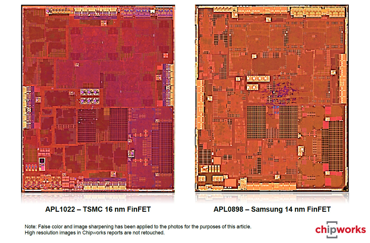
TSMC 16nm+ = 80 * 64 = 5120
Samsung 14nm = 78 * 64 = 4992
Intel 14nm = 70 * 52 = 3640
Samsung 10nm = 3145F
TSMC 10nm = 2662F
Intel 10nm = 54 * ?? = 1820F
TSMC 7nm = 1664F
Samsung / GloFo 7nm = *this post* (the article does not further specify between the two companies)
GloFo - Samsung = "44/48" (don't ask me what this means) gate pitch x 36 interconnect pitch = 1.584 / 1.728
As we already knew, they will use SiGe channel strain.
Edit: As I explain here and here, I now estimate that this simple area estimate will produce an area for Intel's 10nm of
Intel 10nm = 54 * 36 = 1.944
They will be able to get a 1.33x higher logic cell density by aggressive design rule enhancement.
We already knew from a nice find by Ashraf Eassa that TSMC's 7nm HD SRAM will be 0.54x Intel's 14nm SRAM cell at 0.027um^2, and now we also have some new infos about Samsung and GloFo's 7nm dug up by SemiEngineering.
So here's some context first:
Gate pitch (nm) x Interconnect pitch (nm) = Transistor area (nm^2)
Intel 22nm = 90 * 80 = 7200
TSMC 16nm+ = 80 * 64 = 5120
Samsung 14nm = 78 * 64 = 4992
Intel 14nm = 70 * 52 = 3640
Samsung 10nm = 3145F
TSMC 10nm = 2662F
Intel 10nm = 54 * ?? = 1820F
TSMC 7nm = 1664F
Samsung / GloFo 7nm = *this post* (the article does not further specify between the two companies)
GloFo - Samsung = "44/48" (don't ask me what this means) gate pitch x 36 interconnect pitch = 1.584 / 1.728
As we already knew, they will use SiGe channel strain.
Edit: As I explain here and here, I now estimate that this simple area estimate will produce an area for Intel's 10nm of
Intel 10nm = 54 * 36 = 1.944
They will be able to get a 1.33x higher logic cell density by aggressive design rule enhancement.
Last edited: