New Zen microarchitecture details

Page 21 - Seeking answers? Join the AnandTech community: where nearly half-a-million members share solutions and discuss the latest tech.

hojnikb

Senior member
Sep 18, 2014
562
45
91
Bristol Ridge isn't Zen, it's Excavator for the desktop. The reason it is relevant is that it's launching the socket that will be used by Zen. As Bristol Ridge is essentially the same silicon as Carrizo, the 2MB L2 cache is a known entity. From what we've seen from Carrizo, these chips will be a reasonable step up from Kaveri, but still no where near anything Intel is selling in most cases.

since when is it confirmed that carrizo die has only L2 cache in its fullest form ?

AMD could simply disable 2MB of cache for various reasons like yield, power, etc....
 

ShintaiDK

Lifer
Apr 22, 2012
20,378
145
106
since when is it confirmed that carrizo die has only L2 cache in its fullest form ?

AMD could simply disable 2MB of cache for various reasons like yield, power, etc....

If you have to play the "secret disabled L2 block that nobody found yet" game. Then I think you already lost.
 

The Stilt

Golden Member
Dec 5, 2015
1,709
3,057
106
AMD has released the die polyshot of Carrizo and it is clear that there are no disabled L2 blocks.

The situation is not as simple with Bristol Ridge however. While Bristol Ridge is expected to be the exact same design as Carrizo (a refresh), there are some things which does make it appear otherwise.

If you look at the Zauba shipping manifests, you'll see that AMD has shipped AM4 Bristol Ridge prototypes with "2D34E2AGM44AB" and "2D34E1AGM44AB" OPNs.

The last four characters / numbers tell the number of the cores, amount of cache and the design / stepping identifier.

The first "4" stands for four cores, the second "4" for 2048KB L2 per CU and "AB" for BR-A1" design / stepping.

Carrizo based FX-8800P parts meanwhile has OPN of "FM880PAAY43KA", which translates to four cores (4), 1024KB of L2 per CU (3) and CZ-A1 (KA).

Increasing the L2 cache size back to 1MB per core or 2MB per CU would definitely improve the performance of Excavator desings, however even if the change would improve the IPC of Excavator by another 5% what's the point? Making such a change would no doubt cost several millions and still Excavator wouldn't be anywhere close to the competition.
 

dark zero

Platinum Member
Jun 2, 2015
2,655
138
106
AMD has released the die polyshot of Carrizo and it is clear that there are no disabled L2 blocks.

The situation is not as simple with Bristol Ridge however. While Bristol Ridge is expected to be the exact same design as Carrizo (a refresh), there are some things which does make it appear otherwise.

If you look at the Zauba shipping manifests, you'll see that AMD has shipped AM4 Bristol Ridge prototypes with "2D34E2AGM44AB" and "2D34E1AGM44AB" OPNs.

The last four characters / numbers tell the number of the cores, amount of cache and the design / stepping identifier.

The first "4" stands for four cores, the second "4" for 2048KB L2 per CU and "AB" for BR-A1" design / stepping.

Carrizo based FX-8800P parts meanwhile has OPN of "FM880PAAY43KA", which translates to four cores (4), 1024KB of L2 per CU (3) and CZ-A1 (KA).

Increasing the L2 cache size back to 1MB per core or 2MB per CU would definitely improve the performance of Excavator desings, however even if the change would improve the IPC of Excavator by another 5% what's the point? Making such a change would no doubt cost several millions and still Excavator wouldn't be anywhere close to the competition.
In mobile could still give some fight (but going at higher costs), but they are already and finally giving a good bye to Bulldozer and CAT for good.... at least, seems that Bristol Ridge won't use the failed processing of Carrizo... seems also that is getting full 4MB of cache, so expecting to be finally at Phenom II levels, meaning that they would stay be competitive.
 

JDG1980

Golden Member
Jul 18, 2013
1,663
570
136
Increasing the L2 cache size back to 1MB per core or 2MB per CU would definitely improve the performance of Excavator desings, however even if the change would improve the IPC of Excavator by another 5% what's the point? Making such a change would no doubt cost several millions and still Excavator wouldn't be anywhere close to the competition.

Exactly. Why waste money polishing a turd?

It's clear at this point that AMD is betting their future on the upcoming 14nm FinFET products, and 28nm is basically an EOL write-off at this point. It was obvious in mid-2015, when AMD did basically a full year of rebrands with Carrizo and Fiji as their only two new products. If they weren't willing to optimize their mid-range GPUs on 28nm last year (which might actually have produced a competitive product with Maxwell) then why would they waste money optimizing a CPU architecture that definitely won't compete, and that the company wrote off as a "miserable failure" years ago?
 

DrMrLordX

Lifer
Apr 27, 2000
21,582
10,785
136
Actually, 4m XV with L3 probably WOULD be competitive. AMD didn't have the resources to make it a reality for 2015 (when it would have needed to hit the market) while also working on Zen in the background. So they made their choices.
 

IllogicalGlory

Senior member
Mar 8, 2013
934
346
136
As a follow up to the bitsandchips April fool's benchmarks, here's the 50% that's truth:

The news of yesterday was an April's Fool, and at the present moment is not a secret anymore. The AIDA64 screens were fakes, but there is a kernel of truth.

First of all, A0 samples of 8 cores Zen exist, and it seems that AMD has already delivered them to its partners for the preliminary tests. The base frequency seems to be very high (3 GHz, Turbo still not enable with these ES) for a high end 8 cores CPU, also produced on a new node like the 14nm LPP FinFET of Samsung/GloFo (The first ES of Bulldozer worked at 2,8 GHz). It is a promising start.

About Zen, I can tell you some my speculations (NO OFFICIAL INFO) and some news from USA (from the same guy who told me about Zen, 3 days earlier the Official Presentation made by AMD).

If 14nm LPP will be good, Zen base frequency (8 cores version, TDP 95W) will be 3.7-3.8 GHz. Turbo 4.1-4.2 GHz. If 14nm LPP will be very good (or if AMD will commercialize a limited edition, like the Athlon Slot A 1GHz during the good old times), Zen will have a base frequency of 4 GHz (Turbo 4.2-4.3 GHz). Also, the overclockers will have a lot of fun, because of the soldered IHS!

Zen seems to be a High Performance and High Frequency uArch, like Skylake and Kaby Lake, but with some little tweak. The design team lead by Keller, as you know, has chosen to simplify some features in order to limit the Power Consumption and improve the Frequency, due to the low availability of appropriate software at the present moment (e.g. 2 x 128 Bit FMA instead of one big 256 Bit FMA SIMD). FPU units, however, will be very strong. In theory, Zen will be a monster in video games tasks (It's just an example). We can expect an IPC at Broadwell level. And if some companies want some features, AMD can do a Custom Zen CPU/APU (It has a modular design).

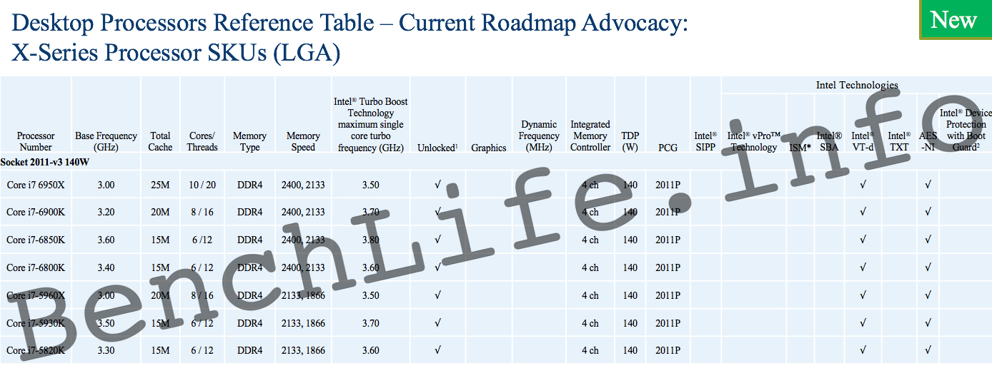
Last, but not the least, the part of the news about Intel was true. It seems that Intel will commercialize a 10 cores Broadwell-E due to its own internal Zen simulations (Intel has some data we don't know, yet, and has skilled engineers that know what they do). Zen will have 8 cores, while Broadwell-E 10 cores. So, Intel will have the “King of the Hill”, but Zen seems to be very good in the mid range of the market (AKA, gaming and enthusiast configurations).

http://www.bitsandchips.it/52-english-news/6815-speculations-about-zen-after-our-april-s-fool

How much of this is true, I can't say, but I'm holding out hope. Overclocker's dream! ;)
 
Last edited:

The Stilt

Golden Member
Dec 5, 2015
1,709
3,057
106
3.7 - 3.8GHz base & 4.1 - 4.2GHz turbo is extremely wishful thinking for a 8C/16T CPU at 95W TDP.

I would be shocked to see anything higher than =< 3.2GHz baseclock @ 95W, if that for the full chip.
 

Abwx

Lifer
Apr 2, 2011
10,854
3,298
136
In its current form GF s 14nm LPP LVT is either 15% more efficient or 20% faster than Intel s 14nm, given that the 14nm LPP sLVT will trade a part of the low static power for higher frequency ceiling those 4GHz+ figures are not even surprising...
 

The Stilt

Golden Member
Dec 5, 2015
1,709
3,057
106
Does anyone happen to know the die size of Broadwell-DE (the 8 core variant)?
 

JDG1980

Golden Member
Jul 18, 2013
1,663
570
136
3.7 - 3.8GHz base & 4.1 - 4.2GHz turbo is extremely wishful thinking for a 8C/16T CPU at 95W TDP.

It would be very difficult to do at 95W, unless AMD managed to pull off a much bigger design coup than anyone suspected. But if they're willing to push the TDP envelope to 140W or so, then it's not out of the question.
 
Mar 10, 2006
11,715
2,012
126
It would be very difficult to do at 95W, unless AMD managed to pull off a much bigger design coup than anyone suspected. But if they're willing to push the TDP envelope to 140W or so, then it's not out of the question.

Even Intel at 140W doesn't hit those kinds of frequencies. The numbers given by the bits 'n chips guy is pure fantasy.
 

JDG1980

Golden Member
Jul 18, 2013
1,663
570
136
Even Intel at 140W doesn't hit those kinds of frequencies.

Not on Haswell-E, not quite, but remember that's 22nm. The 14LPP process that AMD is using is between Intel's 22nm and 14nm processes in terms of feature size, and likely energy efficiency as well.

Even on 22nm, Intel can come pretty close to hitting those clock speeds on 8 cores without blowing up the TDP. Take a look at this analysis from Tom's Hardware. At 100% load, the CPU is only averaging 121W on the 12V rail (including losses from power conversion) with spikes to a maximum of 141W. Intel chose not to go higher than 3.0 GHz with the i7-5960X base clock for a combination of yield and marketing reasons, not TDP limits. Even at 4.0 GHz, the average at 100% load for all 8 cores was 146W (maximum spikes to 165W). Depending on how you define TDP and what your margin of error is, you could easily slap a 145W TDP label on there and it would be defensible.

Now consider that Broadwell-EP (on Intel 14nm) already has a 12-core chip with a base clock of 3.0 GHz. How high can you go in that same TDP envelope if you have only 2/3 the core count? I guess we'll find out when Broadwell-E HEDT parts hit the shelves this summer.
 

deasd

Senior member
Dec 31, 2013
513
724
136
8 cores for mid-range......? So many people wouldn't afford to buy 8 core Zen if what bitsandchips said are true, why call it mid-range product.
But IMO 3.5Ghz for octal-core Zen is pretty likely because ES already hits 3Ghz.
 
Mar 10, 2006
11,715
2,012
126
Not on Haswell-E, not quite, but remember that's 22nm. The 14LPP process that AMD is using is between Intel's 22nm and 14nm processes in terms of feature size, and likely energy efficiency as well.

Even on 22nm, Intel can come pretty close to hitting those clock speeds on 8 cores without blowing up the TDP. Take a look at this analysis from Tom's Hardware. At 100% load, the CPU is only averaging 121W on the 12V rail (including losses from power conversion) with spikes to a maximum of 141W. Intel chose not to go higher than 3.0 GHz with the i7-5960X base clock for a combination of yield and marketing reasons, not TDP limits. Even at 4.0 GHz, the average at 100% load for all 8 cores was 146W (maximum spikes to 165W). Depending on how you define TDP and what your margin of error is, you could easily slap a 145W TDP label on there and it would be defensible.

Now consider that Broadwell-EP (on Intel 14nm) already has a 12-core chip with a base clock of 3.0 GHz. How high can you go in that same TDP envelope if you have only 2/3 the core count? I guess we'll find out when Broadwell-E HEDT parts hit the shelves this summer.

Erm...
broadwell-e.jpg


8C/16T on Intel 14nm is 3.2GHz base/3.7GHz max single core turbo.
 

SK10H

Member
Jun 18, 2015
113
42
101
Unfortunate term for AMD...since we've heard it before near a launch.

Not sure how you manage to twist "overclockers will have a lot of fun, because of the soldered IHS" into "overclockers's dream", and that's not even from an official AMD rep this time.

I am sure overclockers have had enough fun with TIM already. :thumbsdown:
 

LTC8K6

Lifer
Mar 10, 2004
28,520
1,575
126
Not sure how you manage to twist "overclockers will have a lot of fun, because of the soldered IHS" into "overclockers's dream", and that's not even from an official AMD rep this time.

I am sure overclockers have had enough fun with TIM already. :thumbsdown:

It was a quote from a post above...

If you would read all of the posts first, instead of just reacting...
 

deasd

Senior member
Dec 31, 2013
513
724
136
Erm...

8C/16T on Intel 14nm is 3.2GHz base/3.7GHz max single core turbo.

I think the higher TDP is due to LGA2011 implementing quad DDR4 channel, OTOH the 8c version is possible to be crippled from a unhealthy 10c die.

Unfortunate term for AMD...since we've heard it before near a launch.
I don't know why, unfortunate for amd because it can be overclocked??:\
 
Last edited:

LTC8K6

Lifer
Mar 10, 2004
28,520
1,575
126
I think the higher TDP is due to LGA2011 implementing quad DDR4 channel, OTOH the 8c version is possible to be crippled from a unhealthy 10c die.


I don't know why, unfortunate for amd because it can be overclocked??:\

Because the same term, "overclocker's dream", that IllogicalGlory used above, was used to describe Fury video cards. And they were anything but that. :D

How could anyone who frequents this board, or is familiar with the Fury launch, forget that? :)
 
Mar 10, 2006
11,715
2,012
126
I think the higher TDP is due to LGA2011 implementing quad DDR4 channel, OTOH the 8c version is possible to be crippled from a unhealthy 10c die.

How many watts do you suppose those extra two channels gobble up?

Anyway, I think it's probably worth keeping expectations in check around the clock speeds of the 8C/16T 95W Zen chip. It will be a good multithreaded performer most likely but I don't expect particularly high clocks, especially on a mobile-first process. I doubt Samsung had high performance, high frequency CPUs at the top of its mind when it defined and executed 14LPP.

This is a process that was first and foremost aimed at building mobile processors for Apple, Qualcomm, and Samsung System LSI.
 

itsmydamnation

Platinum Member
Feb 6, 2011
2,744
3,079
136
Erm...
broadwell-e.jpg


8C/16T on Intel 14nm is 3.2GHz base/3.7GHz max single core turbo.

So pipeline length of Zen is confirmed 19 stages then? Whats the FO4 target of each core per stage?

There is more to clock speed then process. There is more to power usage then process. In terms of active power process has been playing less and less of a factor each new node. That's why coming up with architectures that work well with dark silicon are so important.

i would not make a serious guess at target clock speed, anything is possible.
 
Mar 10, 2006
11,715
2,012
126
So pipeline length of Zen is confirmed 19 stages then? Whats the FO4 target of each core per stage?

There is more to clock speed then process. There is more to power usage then process. In terms of active power process has been playing less and less of a factor each new node. That's why coming up with architectures that work well with dark silicon are so important.

i would not make a serious guess at target clock speed, anything is possible.

OK, so you think AMD has put together a CPU core with Haswell-class x86 ST perf/clock and will be able to hit much higher clocks in a given power envelope than Intel is seemingly able to with Broadwell?

Is that what you are saying?