Is 10/14nm the max for silicon? Where do we go from here? The end of Moore's Law?

bob4432

Lifer
Sep 6, 2003
11,694
28
91
I will preface this question that I have been into computers pretty heavily from 1995 to about 2010 when I went into embedded systems and the design of multirotor flight controllers as they switched from 8bit to 32bit. Now, in 2017, back to computers and I am reading and seeing 10/14nm a possible wall for silicon.

I was wondering, is 10 or 14nm the max for silicon? If so, is there some other material or hybrid material that can continue Moore's law or is it now @ 10 or 14nm cores and just adding more cores per physical cpu to get the desired effect of more power in the same space, along with other manf abilities to get power per size up?

I know there is a rather small amount of the population (with the exception of Government, R&D and the niche fields that need more power than say a i5-2500K or an i7-2600K, and they probably already have or are working on their needs) that truly needs more processing power, especially on the cpu side, but where do we go from here (as I write this from an old Lenovo T400 laptop w/ 8GB of ram and a SSD, it is a decent laptop for web browsing, lower resolution PS and AI work, smaller assembly SolidWorks design, etc. and when I need a new laptop I will probaby upgrade to a T430 or something around that) As you know, Moore's states approximately every 18mos computational power would double, but if we cannot shrink the transistors and get more per square inch (or square centimeter for the rest of the world), what is your personal opinion as I have been out of normal computers for some time (as you can see from rig in sig)?

Would definitely like to hear from you and educate me about whether I am way off or silicon still does have more life in it, say 7nm or less?

If this has been beat to death already during the times I was away, please point me to the threads if you would be so kind, thanks.

Thanks for your input,
Bob
 
Last edited:

jpiniero

Lifer
Oct 1, 2010
14,600
5,221
136
Intel is already building a fab for 7 nm, so that's going to happen. The foundries are of course playing games with node names but it seems like they will get to at least Intel's 7 nm density eventually.

Remember that Moore's Law is about economics, not what's actually theoretically possible.
 

bob4432

Lifer
Sep 6, 2003
11,694
28
91
Thanks for the info, was not aware of 7nm density. Any idea where silicons max is? Moore's Law 1965-?
 

LightningZ71

Golden Member
Mar 10, 2017
1,627
1,898
136
7mm is going to be around a long time. There are some test labs for 5nm and 4nm, so building a circuit at that feature size is theoretically possible. However, your gate widths are well under 10 atoms at that point, and even manipulating them at that precision is fiendishly difficult. No doubt, there will be a commercially produced chip that features those sizes, but I fear that it will never be economical to mass produce them.

What comes next? Different approaches to computing, greater width 8-10 cores becomes very common, 20+ is in regular use, high performance is north of 32 on the low end. More 3d chips with plenty of thermal vias. Clock speed becomes more important and you see chips pushing north of 5ghz in volume.

After that? No telling.
 

IntelUser2000

Elite Member
Oct 14, 2003
8,686
3,785
136
However, your gate widths are well under 10 atoms at that point, and even manipulating them at that precision is fiendishly difficult..

Gate widths are not at <10 atoms for 5nm nodes. They are far bigger than that.

Intel's feature sizes at 10nm is at 30-50nm depending on what you are looking at. At 5nm the smallest feature size may be at 17nm. That's about 85 atoms.
 

LightningZ71

Golden Member
Mar 10, 2017
1,627
1,898
136
Gate widths are not at <10 atoms for 5nm nodes. They are far bigger than that.

Intel's feature sizes at 10nm is at 30-50nm depending on what you are looking at. At 5nm the smallest feature size may be at 17nm. That's about 85 atoms.

Wait, 17nm, divided by the silicon lattice constant of .5431nm times an FCC packing factor of sqrt(2) is roughly 44 atoms. How's that 85 atoms? I must be missing something here. Though, I agree that even though a given "node" may be advertised as a certain nm size, most features in it will be far larger. However, my point still stands that mass production of 5nm or smaller nodes in economically feasible financials may not be attainable. Just looking at the number of process steps and patterning passes with EUV it takes to turn out what are the first generation 7nm products, 5nm and below may simply take so much time and energy with such a high discard rate that, unless money is almost no object, you won't see it mass produced. And if any feature gets to actually be 5nm, that's 5nm/.5431nm=9 atoms edge to edge, and 13 at sqrt(2) densities(Si).
 

IntelUser2000

Elite Member
Oct 14, 2003
8,686
3,785
136
Wait, 17nm, divided by the silicon lattice constant of .5431nm times an FCC packing factor of sqrt(2) is roughly 44 atoms. How's that 85 atoms? I must be missing something here.

Intel paper noted for a 1.2nm gate oxide its equal to roughly 5 Si atoms. I don't know if the gate oxide is different from a whole transistor in the way its made so the counting becomes different.

http://lampx.tugraz.at/~hadley/nanoscience/week5/Intel_2004.pdf

Though, I agree that even though a given "node" may be advertised as a certain nm size, most features in it will be far larger.

You know why its larger right? The 1.2nm gate oxide on 90nm became ~3nm on 45nm became it was too thin to be practical so they used new material that offered same performance as scaling the size down. The smallest size becomes a limiter to scaling, so they use other tricks to stop that from becoming smaller. Then other parts of the circuit becomes the bottleneck.

Eventually, the whole thing will be too small to scale down at all.

On 10nm Intel is using features like CoAG and less dummy transistors to increase practical density, even though the transistor size stays same.

However, my point still stands that mass production of 5nm or smaller nodes in economically feasible financials may not be attainable.

True.

I think they'll be able to pull few more generations. After that I think all industrialized nations will wake up and realize they put much economic weight behind an industry that isn't going to improve at the rate it did anymore. Maybe they'll get to realize what enough is enough means. Putting computers on every corner of our lives does what?
 

whm1974

Diamond Member
Jul 24, 2016
9,460
1,570
96
What comes next? Different approaches to computing, greater width 8-10 cores becomes very common, 20+ is in regular use, high performance is north of 32 on the low end. More 3d chips with plenty of thermal vias. Clock speed becomes more important and you see chips pushing north of 5ghz in volume.

After that? No telling.
The main problem of increasing the core counts of CPUs it is hard to develop software that can take advantage of the added cores.
 

IntelUser2000

Elite Member
Oct 14, 2003
8,686
3,785
136
What comes next? Different approaches to computing, greater width 8-10 cores becomes very common, 20+ is in regular use, high performance is north of 32 on the low end. More 3d chips with plenty of thermal vias. Clock speed becomes more important and you see chips pushing north of 5ghz in volume.

After that? No telling.

I think clock speed is facing a harder wall than process.

The absolute highest overclock is achieved by AMD's FX processor at a frequency of 8794.33MHz. You'll see the top results are all made by CPUs that sacrificed perf/clock for frequency and are deeply pipelined designs - Bulldozer, Prescott. For Intel the highest ones are based on Celerons. Apparently the Pentiums are too complex to reach that frequency. That's with exotic cooling. Best available, and not at all sustainable for long term use. And most have only 1 core active.

Then there's top air overclocks. I don't know the top. I think its 5.6GHz for all cores.

Interestingly, 5.5GHz was the peak reached for IBM's processor in 2012. They are a bit lower now, at 5GHz. They leaped from 2.3GHz to 5GHz on the Power 6 generation. They went to in-order processing to achieve that, and dropped in frequency a bit when they went back to out of order on the next gen. Power 6 was 2007. Power CPUs use 200W or more though.

Kabylake can also do 5GHz. Coffeelake might do slightly better. 5.2GHz maybe? The pattern seems to be ~5GHz is the point where it takes all effort to reach it. It must be at a point where thermals and power usage goes to the stratosphere.

For a decade, top air clock(including overclocking) haven't budged much from 5GHz. So the clocks are converging to mostly the same point, despite being on a different architecture, different ISA, different process, different company even.

Another thing converging seems to be performance per clock(referred to some folks as IPC). Apple Ax cores. Intel Core lines. AMD Ryzen. IBM Power. They are roughly at the same level.
 
  • Like
Reactions: Edrick

LightningZ71

Golden Member
Mar 10, 2017
1,627
1,898
136
I agree that individual programs are only parrallel-izable to a point in most cases. It's going to be more on the OS to find a way to run more programs at once. Virtualization will be able to be used even more pervasivily with higher and higher core counts and larger L3 caches, better taking advantage of the wider chips. I think that raw performance will give way to higher utilization as the short term focus.

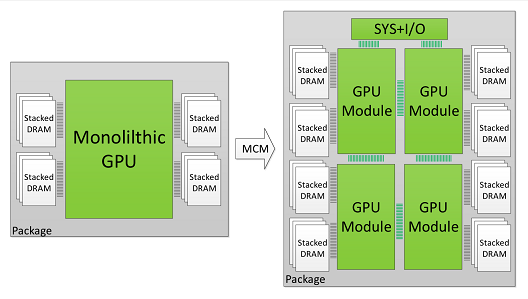
I also think that the chip companies have been working on the lowest hanging fruit with larger caches and more cores. MCM and the related heterogeneous chip module techs will soon give us processors that have chiplets that are optimized for function with respect to process with chiplets that are designed to clock very high for the functions that can take advantage of it, others that are optimized for density like caches etc, and others that are optimized for power efficiency like low speed I/O.

Then, there is always the snake oil called quantum computing...
 

NTMBK

Lifer
Nov 14, 2011
10,237
5,021
136
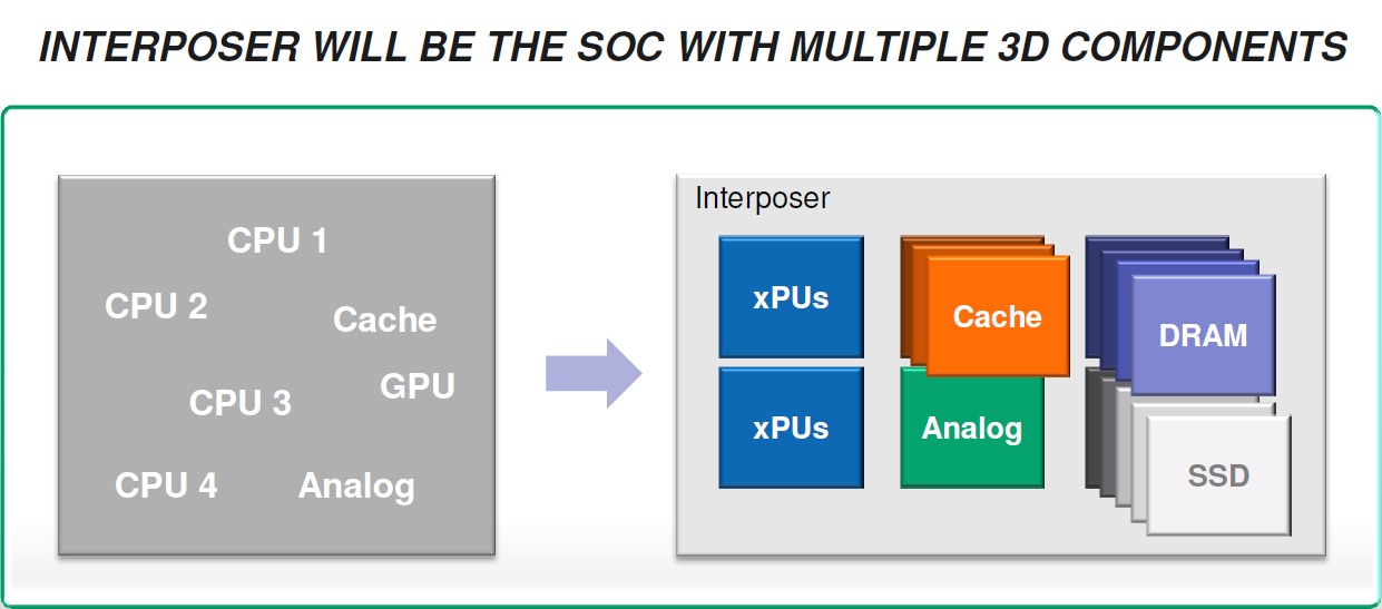
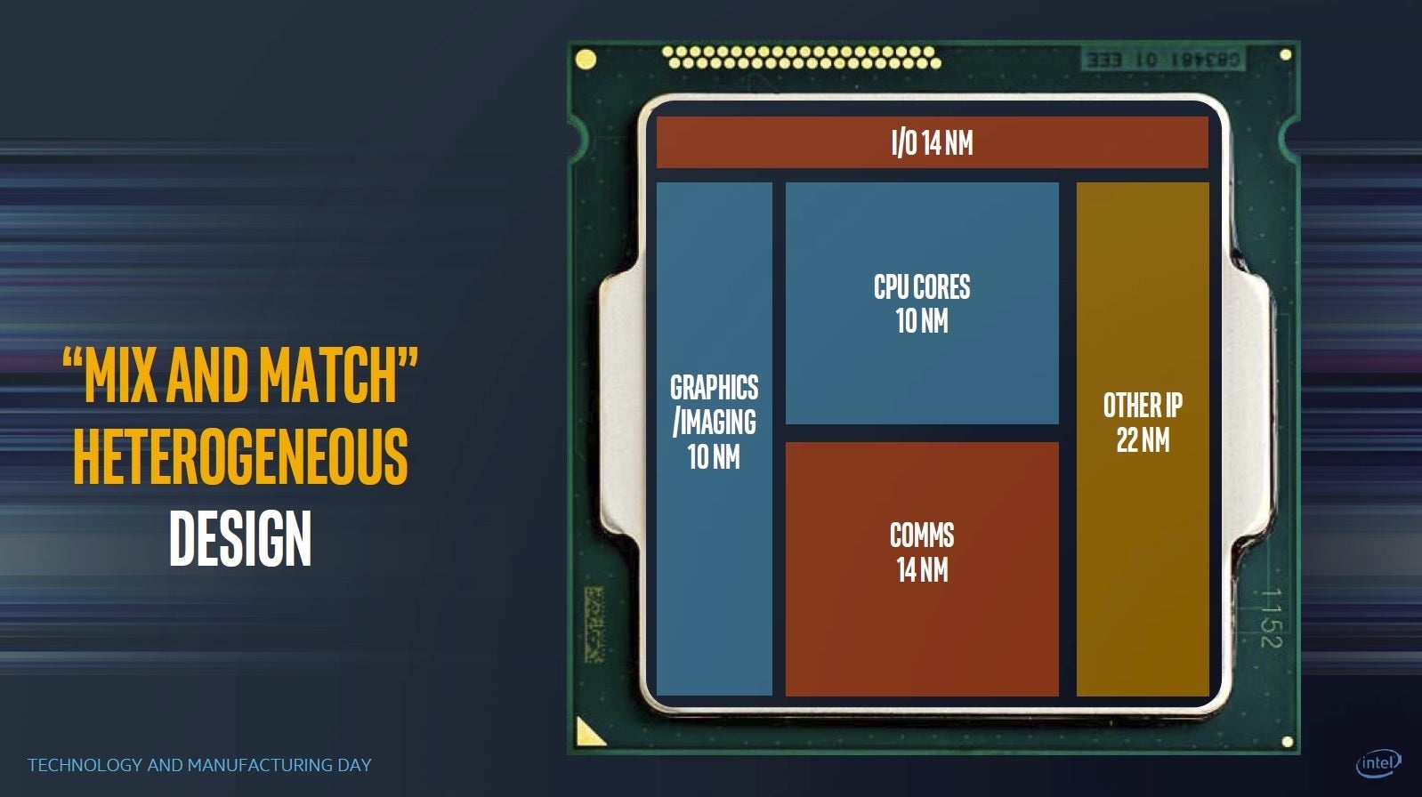
I think we're going to see more use of specialized manufacturing nodes for different components, all integrated onto interposers. The process that can give better density for your GPU is also going to reduce the clock speed of your CPU. Maybe you want your L3 manufactured using a dedicated memory process. Maybe your cutting edge 7nm process is too expensive to use for entire chips, so you put things like the integrated southbridge on an old 14/28nm process.

We saw this in action with AMD's APUs when they went from 32nm PDSOI to 28nm bulk. 28nm let them cram in denser and more efficient GPUs, but the CPU clock speeds went down when they lost SOI. What if they could have used 32nm and 28nm in the same chip instead?

NVidia, AMD and Intel are all looking into it.

AMD-Die-Stacking.jpg


intel_tech_manu_2-100715589-orig.jpg


mcm_0.png
 
  • Like
Reactions: Christopher Bohling

tommo123

Platinum Member
Sep 25, 2005
2,617
48
91
re: ^ what's the diff between interposers and vias? are vias the connectors between layers of chips?
 

maddie

Diamond Member
Jul 18, 2010
4,740
4,674
136
Don't be stuck on Silicon. It's all about costs and prices. When Silicon begins to stall out completely, then R&D will increase significantly on alternatives which DO exist. GaAs. nanotubes,etc. Do we really think that the companies will concede defeat and forever eschew advancement with the monetary gains?

With interposers in the mix, all materials & processes can be mixed as deemed best.
 
  • Like
Reactions: pjmssn

dbcoopernz

Member
Aug 10, 2012
68
4
71
Don't be stuck on Silicon. It's all about costs and prices. When Silicon begins to stall out completely, then R&D will increase significantly on alternatives which DO exist. GaAs. nanotubes,etc. Do we really think that the companies will concede defeat and forever eschew advancement with the monetary gains?

With interposers in the mix, all materials & processes can be mixed as deemed best.

Much easier said than done. Look at how long it took to introduce a material change as simple as FDSOI.
 

dullard

Elite Member
May 21, 2001
25,068
3,416
126
re: ^ what's the diff between interposers and vias? are vias the connectors between layers of chips?
Yes, vias are the connectors between layers on a printed circuit board. A very simple PCB will have copper on both sides of a non-conductive base. In order to get an electric connection between the copper on top and the copper on bottom, a via is made. A via is a drilled hole, lined with conductive material (usually electroplating, but it could be a metal tube, rivet, or similar way to conduct electricity from one side of the hole to another). Since it was mentioned above, a thermal via is intended to conduct heat from one copper layer to another through a hole and metal filling just like electricity conducts through a via.

An interposer is a very simple PCB designed to connect two or more different devices. An interposer may have a few electronic components on it, but often, it just is as basic of a PCB as possible consisting of just electrical connections. You could almost think of an interposer as a miniature motherboard where distinct chips get soldered onto it.

Interposers are often used to connect things of different pitch. For example, a CPU may need thousands of connections to the motherboard, but the CPU is too small to have thousands of tiny reliable pins / balls to connect to the motherboard. A CPU that small can only reliably be made with a solder connection. So, you solder a small CPU onto a large interposer to spread out the necessary pins. Then you have a CPU+Interposer that people can insert/remove/upgrade at will without any additional solder.
 

maddie

Diamond Member
Jul 18, 2010
4,740
4,674
136
Yes, vias are the connectors between layers on a printed circuit board. A very simple PCB will have copper on both sides of a non-conductive base. In order to get an electric connection between the copper on top and the copper on bottom, a via is made. A via is a drilled hole, lined with conductive material (usually electroplating, but it could be a metal tube, rivet, or similar way to conduct electricity from one side of the hole to another). Since it was mentioned above, a thermal via is intended to conduct heat from one copper layer to another through a hole and metal filling just like electricity conducts through a via.

An interposer is a very simple PCB designed to connect two or more different devices. An interposer may have a few electronic components on it, but often, it just is as basic of a PCB as possible consisting of just electrical connections. You could almost think of an interposer as a miniature motherboard where distinct chips get soldered onto it.

Interposers are often used to connect things of different pitch. For example, a CPU may need thousands of connections to the motherboard, but the CPU is too small to have thousands of tiny reliable pins / balls to connect to the motherboard. A CPU that small can only reliably be made with a solder connection. So, you solder a small CPU onto a large interposer to spread out the necessary pins. Then you have a CPU+Interposer that people can insert/remove/upgrade at will without any additional solder.

I find your explanation a bit misleading. The term interposer used here, I'm thinking, means silicon interposer.

"For example, a CPU may need thousands of connections to the motherboard"
Don't you mean to other ICs? Traditionally the only way to connect ICs was through the PCB which has a low limit. Now with interposers, this # can be greatly increased. In other words there is still no 1000's of connections to the motherboard with an interposer. The various ICs needing 1000's of pathways all reside on the interposer.

"but the CPU is too small to have thousands of tiny reliable pins / balls to connect to the motherboard"
Not that the CPU is too small, but the connection density limit on PCBs is too low to support that density? After all the HBM2 modules have thousands of connections on a 100mm^2 area using microbumps. The GPUs they connect to also have a similar #.

Also interposers have a very low latency on the order of 1ns, a much lower value than a PCB connection. This was gotten from a Xilink slide.
 

R0H1T

Platinum Member
Jan 12, 2013
2,582
162
106
Don't be stuck on Silicon. It's all about costs and prices. When Silicon begins to stall out completely, then R&D will increase significantly on alternatives which DO exist. GaAs. nanotubes,etc. Do we really think that the companies will concede defeat and forever eschew advancement with the monetary gains?

With interposers in the mix, all materials & processes can be mixed as deemed best.
Graphene!
 

dullard

Elite Member
May 21, 2001
25,068
3,416
126
Not that the CPU is too small, but the connection density limit on PCBs is too low to support that density? After all the HBM2 modules have thousands of connections on a 100mm^2 area using microbumps. The GPUs they connect to also have a similar #.
I think we have a definition misunderstanding. For a given needed number of connections, a small chip (my words) is equivalent to a high density (your words).

Yes, those chips can have microbumps with very high density. But microbump products have problems. For example, they are not readily user-swappable. You don't just pull up a GPU chip and put in a new GPU chip. The microbumps are too small and too dense to do that without proper equipment. You are correct that the CPU is not too small to have connections, but the CPU is too small to have connections that are low enough in density to be directly user-replaceable.

An interposer is often used as a way to convert high density connections to low density ones. With an interposer, a user can swap out a high density chip because the interposer gives them a low density connection method with strong, sizable, and (usually) sturdy connection points. Just look at this typical interposer design with high density connections on top and lower density connections on bottom:

https://en.wikipedia.org/wiki/High_Bandwidth_Memory#/media/File:High_Bandwidth_Memory_schematic.svg

There are other uses of interposers too. An interposer can also reroute pin layouts. So a company could produce many different chips with different layouts and just have interposers to allow all of those chips to use the same socket. Or an interposer can be used to connect chips produced with incompatible methods that can't be built in one piece. Etc.
 

NTMBK

Lifer
Nov 14, 2011
10,237
5,021
136
Yes, vias are the connectors between layers on a printed circuit board. A very simple PCB will have copper on both sides of a non-conductive base. In order to get an electric connection between the copper on top and the copper on bottom, a via is made. A via is a drilled hole, lined with conductive material (usually electroplating, but it could be a metal tube, rivet, or similar way to conduct electricity from one side of the hole to another). Since it was mentioned above, a thermal via is intended to conduct heat from one copper layer to another through a hole and metal filling just like electricity conducts through a via.

An interposer is a very simple PCB designed to connect two or more different devices. An interposer may have a few electronic components on it, but often, it just is as basic of a PCB as possible consisting of just electrical connections. You could almost think of an interposer as a miniature motherboard where distinct chips get soldered onto it.

Interposers are often used to connect things of different pitch. For example, a CPU may need thousands of connections to the motherboard, but the CPU is too small to have thousands of tiny reliable pins / balls to connect to the motherboard. A CPU that small can only reliably be made with a solder connection. So, you solder a small CPU onto a large interposer to spread out the necessary pins. Then you have a CPU+Interposer that people can insert/remove/upgrade at will without any additional solder.

Sorry, I should have been more explicit that I was talking about silicon interposers enabling die-to-die communication, not just regular interposers used for routing pins.
 

brag.yondide

Junior Member
Jul 8, 2013
14
0
66
...What comes next? Different approaches to computing, greater width 8-10 cores becomes very common, 20+ is in regular use, high performance is north of 32 on the low end...
Depends on what you mean by 'computing', I think.

The von Neumann architecture has been around for greater than half a century. Improvements in semiconductor manufacturing have provided easy gains for the last 40 years. There is a huge trained workforce for producing software for the current computing paradigm. All of which provides an irresistible inertia for maintaining that paradigm.

However, with silicon manufacturing hitting a wall and new technologies yet to mature, we will be forced to step back and re-examine fundamental computing architectures seriously if progress is to continue.

My own guess is that there will be a better definition of fundamental functional (computing) blocks which can then be optimized and combined as needed to achieve higher level functions. This is already happening and will accelerate, I think. (I've always been baffled by why I have the same general purpose computer at home as I do at work when their uses are so different.) For instance, the smart phone SoC isn't really a general purpose computer - it's a UI connected to a radio, Google Home is basically a voice recognition processor connected to a search engine, there are more transistors in your GPU than CPU - come to that, more in the memory than CPU, etc. The technology for combining functional blocks is maturing quickly; the definition of them needs more work, I think.

Best thread here for ages, BTW...
 
Oct 19, 2006
194
1
81
Along with what others have suggested, I think we will see quite a bit more investment in different areas of efficiency, like when GPU's were stuck at 28nm for two generations. Chip designers can focus on making the logic more power efficient or provide more IPC for instance. Logic can be more or less dense, cache sizes and types can be tuned, branch predictors refined, drop legacy x86 ISA, Etc... I can't imagine that any CPU designed so far could not withstand some improvement...
 

PeterScott

Platinum Member
Jul 7, 2017
2,605
1,540
136
I will preface this question that I have been into computers pretty hard from 1995 to about 2010 when I went into embedded systems and the design of multirotor flight controllers as they switched from 8bit to 32bit. Now, back in 2017, I am reading and seeing 10/14nm a possibly a wall.

General usage CPUs already hit the performance wall almost a decade back. Transistor densities kept going up, while CPU performance was stagnant. So I don't see a big deal about Moore's law slowly grinding to a halt as far as general purpose CPUs go. For general purpose CPUs, transistor density increases have stopped driving performance gains anyway, and the performance that is there is largely underutilized.

As you noted: "I know there is a rather small amount of the population (with the exception of Government, R&D and the niche fields that need more power than say a i5-2500K or an i7-2600K"

Niche fields that require big computing resources almost always have highly parallel problems that can respond to just throwing more hardware at the solutions, and the money to do it.

So for CPUs. Yes, Moores law appears to be be grinding down, but it hardly matters.

For gaming GPUs, this is more of a problem as they can utilize every transistor thrown at the problem.
 

Qwertilot

Golden Member
Nov 28, 2013
1,604
257
126
Well, the one thing it has been doing is pushing the power needed to be 'fast enough' down & down over time. It'd have been nice for that to keep going another decade or so I suppose. Oh well :)
 

IntelUser2000

Elite Member
Oct 14, 2003
8,686
3,785
136
General usage CPUs already hit the performance wall almost a decade back. Transistor densities kept going up, while CPU performance was stagnant

For gaming GPUs, this is more of a problem as they can utilize every transistor thrown at the problem.

We have Desktops with 4K monitors, graphics that rival the best 3D quality of $200 million movies just a couple of years ago,

Laptops that were dreamed of by mobile professionals a decade ago can be obtained rather affordably from many manufacturers,

Devices that can fit into your pocket, but is also a computer. Some have reached a price point so low that in countries where people are starving, they have mobile service and a Smartphone capable of taking advantage of Data services!

We are actually at the peak of computing. It might as well be the "Golden Age". Interesting it coincides with the time when the rate of advancement has more or less passed its peak not too long ago.


I think it should be celebrated, rather than put our hands up in despair.