Discussion Intel Nova Lake in H2-2026: Discussion Threads

Page 53 - Seeking answers? Join the AnandTech community: where nearly half-a-million members share solutions and discuss the latest tech.

Geddagod

Golden Member
Dec 28, 2021
1,617
1,665
106
This is just a speculation on my part, but I think there was more to the delay than a packaging issue.

It seems to me that from an array of excuses Intel narrowed down to one that would result in the least PR damage, and it is packaging.

People might think of it like Santa having this phenomenal present in the sled, but he can't deliver it because Santa is out of the red ribbons to tie around the package.
Yeah, I used to claim it was just packaging issues too, but the PTL launch fiasco is so bad (btw Intel is claiming they have that one PTL sku out already lmao) it makes me think 18A is just chopped and that also played a part in the delays.
Even if the CLF die itself is small, binning for power might just be terrible.
Maybe Intel didn't want a repeat of ICL, where ICL server skus had very little to no perf/watt increase over iso core count 14nm skus.
 
  • Like
Reactions: Joe NYC

Joe NYC

Diamond Member
Jun 26, 2021
3,951
5,485
136
Yeah, I used to claim it was just packaging issues too, but the PTL launch fiasco is so bad (btw Intel is claiming they have that one PTL sku out already lmao) it makes me think 18A is just chopped and that also played a part in the delays.
Even if the CLF die itself is small, binning for power might just be terrible.
Maybe Intel didn't want a repeat of ICL, where ICL server skus had very little to no perf/watt increase over iso core count 14nm skus.

The reason I think Intel used packaging as a good excuse because it worked last year. Intel said that packaging was a bottleneck which limited the number of Meteor Lake CPUs could be sold to customers (last year). Which is likely that it was true.

But this time, it just does not feel like everything was ready, and Clearwater Forrest would already be in volume shipments today were it not for a tiny issue with packaging...

Binning of CPU dies might be an issue, or it could just be that the verification was just not quite there to allow volume production shipments.
 

Khato

Golden Member
Jul 15, 2001
1,328
398
136
Again, CWF is Intel's first product using Foveros Direct packaging.

Why do you think that AMD waited over a year to released the stacked cache variants of zen3? It was all part of the original design... they were just waiting for TSMC to iron out the kinks with the process to a point where the processors wouldn't self destruct an order of magnitude or two faster than raptor lake.

It's that much worse for Intel because they're not just putting some extra cache on top, aka attaching two die together. They're attaching 3 compute die to an active base die. An 80% success rate for each attachment yields 80% success with AMD's simple approach... and roughly 50% success with CWF.
 

511

Diamond Member
Jul 12, 2024
5,120
4,605
106
Yeah, I used to claim it was just packaging issues too, but the PTL launch fiasco is so bad (btw Intel is claiming they have that one PTL sku out already lmao) it makes me think 18A is just chopped and that also played a part in the delays.
They are shipping PTL to OEMs from Oregon dev Fab and it takes time for that SKU to be converted into a laptop it's not desktop where you can ship it to consumer through channel directly it's their first 3D Bonding process it's entirely possible to have Clearwater Forest with packing delays.
Even if the CLF die itself is small, binning for power might just be terrible.
Maybe Intel didn't want a repeat of ICL, where ICL server skus had very little to no perf/watt increase over iso core count 14nm skus.
this is totally baseless claim for CLF they are not targetting client level clockspeed of 3.5 Ghz+ on E cores
 
  • Like
Reactions: DKR

Geddagod

Golden Member
Dec 28, 2021
1,617
1,665
106
They are shipping PTL to OEMs from Oregon dev Fab and it takes time for that SKU to be converted into a laptop it's not desktop where you can ship it to consumer through channel directly
When Intel launched MTL, they held the launch event before the end of the year, and had laptops out available to buy by the end of the year too. The turn around was insanely quick. LNL deff fulfilled that category.
And those were the two products Intel compared how PTL launch would look like.

Intel just missed PTL launch schedule, badly. From mid 2025 to late 2025 to not showing up till 2026.
this is totally baseless claim for CLF they are not targetting client level clockspeed of 3.5 Ghz+ on E cores
I'm not talking about ICL client, I'm talking about ICL server.
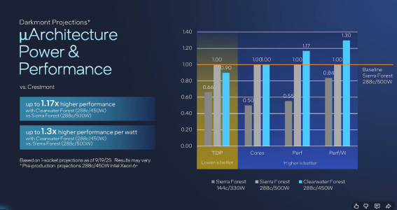
Perf/watt only matched 14nm parts. This would be like 288 clearwater forest parts being only as performant as 288 core sierra forest parts.
Though I will say the current 17% perf bump between the two products is kinda unimpressive.
Intel 10nm+ must have had decent defect density, given they shipped massive ICL dies, but parametric binning was unimpressive. Not just Fmax, but perf/watt too.
 
  • Like
Reactions: Thunder 57

Geddagod

Golden Member
Dec 28, 2021
1,617
1,665
106
Again, CWF is Intel's first product using Foveros Direct packaging.

Why do you think that AMD waited over a year to released the stacked cache variants of zen3? It was all part of the original design... they were just waiting for TSMC to iron out the kinks with the process to a point where the processors wouldn't self destruct an order of magnitude or two faster than raptor lake.

It's that much worse for Intel because they're not just putting some extra cache on top, aka attaching two die together. They're attaching 3 compute die to an active base die. An 80% success rate for each attachment yields 80% success with AMD's simple approach... and roughly 50% success with CWF.
It's very believable that Intel had delays with packaging. But it's also pretty believable they also had issues on 18A too. Intel would rather blame packaging though.

But also, Intel has had how many generations of foveros in mass production so far? And how much later are they launching 3D hybrid bonding than TSMC?
TSMC in comparison didn't seem to have nearly as much experience/volume in 3D stacked advanced packaging as Intel has had before they launched X3D.
 

511

Diamond Member
Jul 12, 2024
5,120
4,605
106
I'm not talking about ICL client, I'm talking about ICL server.
Perf/watt only matched 14nm parts. This would be like 288 clearwater forest parts being only as performant as 288 core sierra forest parts.
Though I will say the current 17% perf bump between the two products is kinda unimpressive.
Intel 10nm+ must have had decent defect density, given they shipped massive ICL dies, but parametric binning was unimpressive. Not just Fmax, but perf/watt too.
1764838774147.png

1.3X perf/watt is decent gen on gen improvement (i have big doubt on intel botching L3 here as well cause consumer Skymont was way ahead even iso power ). I don't think it will be untill DMR the Mesh will be fixed
 
  • Like
Reactions: DKR

rainy

Senior member
Jul 17, 2013
523
453
136
View attachment 134752

1.3X perf/watt is decent gen on gen improvement (i have big doubt on intel botching L3 here as well cause consumer Skymont was way ahead even iso power ). I don't think it will be untill DMR the Mesh will be fixed

I fully understand that you're an Intel foot soldier but please be reasonable: since when marketing slides of any company are unquestionable truth?

Btw, on this slide you've clearly missed Intel famous "up to" phrase which means that 17/30 percent is best case scenario.
 

511

Diamond Member
Jul 12, 2024
5,120
4,605
106
I fully understand that you're an Intel foot soldier but please be reasonable: since when marketing slides of any company are unquestionable truth?

Btw, on this slide you've clearly missed Intel famous "up to" phrase which means that 17/30 percent is best case scenario.
1st i am not a foot soldier 2nd these are the stuff that @Geddagod quoted his numbers from and we don't have any 3rd party benchmark from any company so we don't have any option either way for now
 
  • Haha
Reactions: Thibsie

eek2121

Diamond Member
Aug 2, 2005
3,458
5,105
136
I fully understand that you're an Intel foot soldier but please be reasonable: since when marketing slides of any company are unquestionable truth?

Btw, on this slide you've clearly missed Intel famous "up to" phrase which means that 17/30 percent is best case scenario.
Yep, the “up to” basically means it could be anything, but in at least one workload, they saw X, and in a possibly different workload they saw Y.
 

Geddagod

Golden Member
Dec 28, 2021
1,617
1,665
106
1.3X perf/watt is decent gen on gen improvement
It looks a good bit better than it actually is because of the lowered TDP.
If you increase the TDP to 500 watts, I doubt CLF is much more than a 20% bump in perf/watt.
Meaning most of the improvement should be coming from the node jump itself.
I don't think it will be untill DMR the Mesh will be fixed
If DMR is 256 cores, don't you still end up with the same 128 core stops? Still seems problamatic to me.
 

511

Diamond Member
Jul 12, 2024
5,120
4,605
106
If DMR is 256 cores, don't you still end up with the same 128 core stops? Still seems problamatic to me.
DMR is rome style Mesh each 64 Core Compute tile gets separate mesh of 32 stops not a big large mesh and a big single IO Die on Intel 3/4
 

Geddagod

Golden Member
Dec 28, 2021
1,617
1,665
106
DMR is rome style Mesh each 64 Core Compute tile gets separate mesh of 32 stops not a big large mesh and a big single IO Die on Intel 3/4
That does sound better. AMD's Venice Dense CCDs are supposed to be 32 core stops as well. Going to be interesting to see the bandwidth comparisons between the two.
 

Joe NYC

Diamond Member
Jun 26, 2021
3,951
5,485
136
DMR is rome style Mesh each 64 Core Compute tile gets separate mesh of 32 stops not a big large mesh and a big single IO Die on Intel 3/4

No LLC die stacking, like Clearwater Forrest?

And 64 core die is going to be quite big...
 

Joe NYC

Diamond Member
Jun 26, 2021
3,951
5,485
136
There is die stacking

Well it only contains core+l2 like Clearwater forest as for die size difficult to guess.

So L3 then on a separate die, and the L3 die is equal size in size to the compute die?
 

Supermecha

Junior Member
Nov 9, 2025
2
1
36
Again, CWF is Intel's first product using Foveros Direct packaging.

Why do you think that AMD waited over a year to released the stacked cache variants of zen3? It was all part of the original design... they were just waiting for TSMC to iron out the kinks with the process to a point where the processors wouldn't self destruct an order of magnitude or two faster than raptor lake.

It's that much worse for Intel because they're not just putting some extra cache on top, aka attaching two die together. They're attaching 3 compute die to an active base die. An 80% success rate for each attachment yields 80% success with AMD's simple approach... and roughly 50% success with CWF.
Isn't Ponte Vecchio a more advanced chip than CWF. AMD went from a simple stacked cache on Zen3 to the complex packaging of the MI300 without much fuss. Why is Intel still struggling with CWF's packaging.
 
  • Like
Reactions: booklib28

511

Diamond Member
Jul 12, 2024
5,120
4,605
106
Isn't Ponte Vecchio a more advanced chip than CWF. AMD went from a simple stacked cache on Zen3 to the complex packaging of the MI300 without much fuss. Why is Intel still struggling with CWF's packaging.
In terms of packing yes it's way complicated than MI300 in terms of Tiles usage MI300 has Hybrid bonding alongside CoWoS -S while PVC has Foveros which is similar to CoWoS-S and EMIB which is similar to CoWoS-L
 
  • Like
Reactions: DKR and Joe NYC

511

Diamond Member
Jul 12, 2024
5,120
4,605
106
True I forgot about that. Plus AVX-512 extension should add some extra area too.
well PNC will likely be smaller than 3mm2 for the Core+L1 Considering CGC is almost less than this without AMX ofc i think
 

Khato

Golden Member
Jul 15, 2001
1,328
398
136
Hard to tell. More packaging in general, but no hybrid bonding.
Exactly, it's the hybrid bonding that's the sticking point.

Conceptual simplification of EMIB and Foveros 2.5D is that they're the same as normal FCBGA packaging, just using a silicon substrate instead of an organic substrate. Using silicon enables the finer pitch both because of matched thermal expansion coefficient and the relative ease of making fine wires/pads on silicon. But it's still a solder connection between the pads.

Foveros direct requires getting the two die perfectly flat and aligned such that the pressure/heat of the process bonds copper to copper and dielectric to dielectric. If there's any gaps in that bond electromigration can occur and you'll have raptor lake * 100. Which is again more of a problem with Intel's design because they have all the power hungry core logic on top rather than the power sipping cache.
 
  • Like
Reactions: Elfear