Nah, he bashes Intel for a living.You argue on forums for a living?
Also, 3.7-3.9ghz is indeed the final clock for Gracemont.
-
We’re currently investigating an issue related to the forum theme and styling that is impacting page layout and visual formatting. The problem has been identified, and we are actively working on a resolution. There is no impact to user data or functionality, this is strictly a front-end display issue. We’ll post an update once the fix has been deployed. Thanks for your patience while we get this sorted.
You are using an out of date browser. It may not display this or other websites correctly.
You should upgrade or use an alternative browser.
You should upgrade or use an alternative browser.
Discussion Intel current and future Lakes & Rapids thread
Page 500 - Seeking answers? Join the AnandTech community: where nearly half-a-million members share solutions and discuss the latest tech.
You explicitly claimed that Atom would reach nowhere near 4GHz, even overclocked. Increasingly looks like we're getting 3.9GHz out of the box. Same applies for the IPC uplift.
There s no data published that is related to small cores IPC, so how do you estimate any uplift if ever there s one..?.
What official numbers?
That presentation from yesterday. You didn't even bother to look at the slides before calling them all fake?
There s no data published that is related to small cores IPC, so how do you estimate any uplift if ever there s one..?.
Regarding the IPC comment, I meant his "skepticism" that Atom could come near Core.
That presentation from yesterday. You didn't even bother to look at the slides before calling them all fake?
LOL, what numbers? It was all marketing fluff. There was not a single actual spec in the entire presentation.
Nah, he bashes Intel for a living.
Actually that is correct, I do work at one of the companies doing silicon design that is putting Intel out to pasture.
coercitiv
Diamond Member
Just to make sure: you want to know why it would be impossible for Gracemeont to have almost Golden Cove PPC?!Why would that be impossible again?
LOL, what numbers? It was all marketing fluff. There was not a single actual spec in the entire presentation.
So you even deny that numbers were presented, despite being right there in black and white. At this point you're not even trying to hide the trolling.
And when Gracemont inevitably hits around 4GHz, will you retract all of your past claims to expertise?
dullard
Elite Member
Gracemont performance will surprise you. That is the thing: it isn't a "little" core.It's not included in the graph, unless you think Gracemont has a ~35%+ PPC advantage over Skyalke. (that would be almost Golden Cove PPC)
So you even deny that numbers were presented, despite being right there in black and white. At this point you're not even trying to hide the trolling.
And when Gracemont inevitably hits around 4GHz, will you retract all of your past claims to expertise?
Point out to any real numbers in the midst of that fluff. I want to see what you consider a real data point.
And no, I will always know more about silicon engineering than you, forever. Sorry.
Gracemont performance will surprise you. That is the thing: it isn't a "little" core.
It's not going to be above GLC except at very low power. But it doesn't need to when you get like twice the throughput PPA.
insertcarehere
Senior member
Your original argument: Gracemont cannot possibly have 35+% PPC advantage over Skylake "Almost Golden Cove PPC"
Me: Shows graph where existing smaller cores from other vendors are already approaching ~35% PPC advantage over Skylake
Your reply:
I won't bet on Gracemont actually hitting that mark, but 15-20% PPC advantage over Skylake for Gracemont doesn't seem particularly far fetched at all.
Me: Shows graph where existing smaller cores from other vendors are already approaching ~35% PPC advantage over Skylake
Your reply:
Just to make sure: you want to know why it would be impossible for Gracemeont to have almost Golden Cove PPC?!
I won't bet on Gracemont actually hitting that mark, but 15-20% PPC advantage over Skylake for Gracemont doesn't seem particularly far fetched at all.
Last edited:
dullard
Elite Member
No, not above. But it isn't as much behind in performance as people think either.It's not going to be above GLC except at very low power. But it doesn't need to when you get like twice the throughput PPA.
Point out to any real numbers in the midst of that fluff. I want to see what you consider a real data point.
And no, I will always know more about silicon engineering than you, forever. Sorry.
So first they didn't show any numbers, and now they're not "real" because you're unwilling to accept them. What a surprise.
And I'll be more than happy to use your claims about Gracemont as a demonstration of your ignorance about anything silicon engineering. Care to double down again on your 4GHz claim?
There you go making stuff up again. There are literally no numbers there. It's all fluff and I said so right from the get-go.
By the way, if you are really as good at silicon engineering as you think, the market is incredibly hot for silicon engineers right now. $300k+/year even outside Bay Area for mid-seniority roles. Why not get paid instead of running your mouth on the internet?
There you go making stuff up again. There are literally no numbers there.
Here you go, numbers. Just one example.
And if you go to the source. E.g.
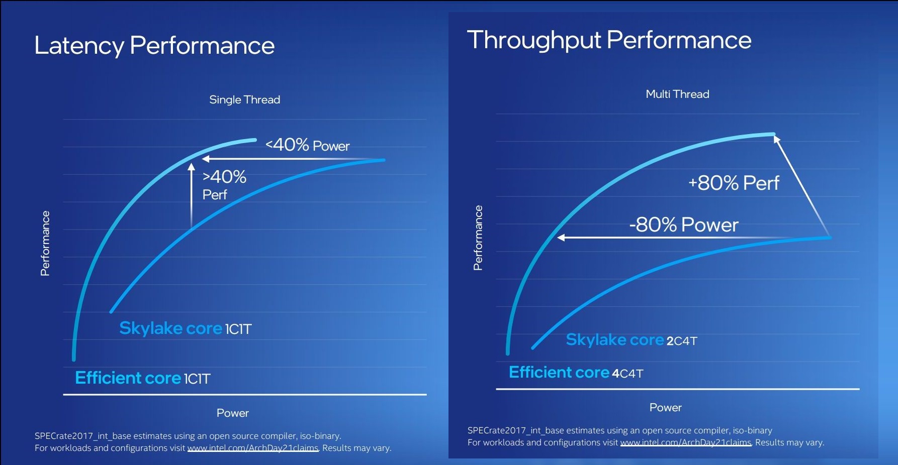
If we compare our Efficient-core to a single Skylake core for a single logical process, we deliver the same performance while consuming less than 40% of the power.
Alternatively, a Skylake core would consume 2.5X more power to achieve the same performance as our Efficient-core.
By the way, if you are really as good at silicon engineering as you think, the market is incredibly hot for silicon engineers right now. $300k+/year even outside Bay Area for mid-seniority roles. Why not get paid instead of running your mouth on the internet?
And why are you assuming I'm not? Probably doing better than an "engineer" who thinks process scaling is a myth, lol.
dullard
Elite Member
Psst: dmens always moves the goal post. He asks for numbers, then claims that the numbers are not what he really wants. He'll come back saying without labels on the axis, the graphs are meaningless. He couldn't make it during his stint at Intel and is now pissed at Intel.Here you go, numbers. Just one example.
And why are you assuming I'm not? Probably doing better than an "engineer" who thinks process scaling is a myth, lol.
Here you go, numbers. Just one example.
And why are you assuming I'm not? Probably doing better than an "engineer" who thinks process scaling is a myth, lol.
Well, I already pointed out the fatal flaw with this claim earlier. Try rebutting that example instead of falling a fluff slide without the slightest bit of salt.
Well, I already pointed out the fatal flaw with this claim earlier
That flaw being what? Your inability to accept the numbers? The same numbers you were just claiming didn't exist?
That flaw being what? Your inability to accept the numbers? The same numbers you were just claiming didn't exist?
Sigh. I'll repeat it once on a Friday. The flaw is that graph is that it fails to specify the perf at iso-power comparison, or the power draw at iso-perf comparison. If the comparison is done at an operating point which grossly favors one design, then it is extremely misleading, and you cannot extrapolate that comparison to other operating points.
This is basic stuff, I know you don't do silicon engineering professionally because it is such a blatantly obvious flaw. It is the kind of thing I would ask a new grad during an interview as an intro question so I don't waste my time.
Here you go, numbers. Just one example.
And if you go to the source. E.g.
And why are you assuming I'm not? Probably doing better than an "engineer" who thinks process scaling is a myth, lol.
There s no perf data here, only a perf/watt comparison blurred by the fact that there s a new process at work.
As already said a shrinked SKL would reproduce the first graph, it would gain close to 40% better perf at isopower.
For the second graph a shrinked SKL would use 50% less power, stick two cores together and they ll exhibit 100% more perf at isopower..
Also, at the risk of repeating myself you should take notice of the bench wich is Spec_rate and not Spec_int.
dullard
Elite Member
So, if you shrinked the process size, you'd get close to 40% better, Gracemont is close to 40% better with a process node shrink, so I'm supposed to conclude that the Gracemont data is fake? I'm not quite following. It is almost as if you proved the opposite of what you wanted to prove.As already said a shrinked SKL would reproduce the first graph, it would gain close to 40% better perf at isopower.
So, if you shrinked the process size and used double the cores, you'd get close to 100% better, Gracemont is close to 80% better with a process node shrink and 2 cores (not quite 100% because it is Atom-based after all), so I'm supposed to conclude that the Gracemont data is fake? I'm not quite following. It is almost as if you proved the opposite of what you wanted to prove.For the second graph a shrinked SKL would use 50% less power, stick two cores together and they ll exhibit 100% more perf at isopower..
Diminishing returns apply for anything that increases size or power. If making a cache 2x bigger increases performance by 'y' then another doubling does not mean you are now getting '2y' more performance.
But I think that is the rule of thumb. But it is not apparent when you go from 1 to 2 that the one of the variables is linear and the other is exponential. as in:
1x -> 1y
2x -> 2y
4x -> 3y
8x -> 4y
So there are diminishing returns, when for each 1 unit of performance increase you have to double the die area.
The flaw is that graph is that it fails to specify the perf at iso-power comparison, or the power draw at iso-perf comparison.
The numbers they have both spoken and on their source website are very clear, but you evidently didn't even look at them.
If we compare our Efficient-core to a single Skylake core for a single logical process, we deliver 40% more performance at the same power.
If we compare our Efficient-core to a single Skylake core for a single logical process, we deliver the same performance while consuming less than 40% of the power.
Alternatively, a Skylake core would consume 2.5X more power to achieve the same performance as our Efficient-core.
If we compare four of our new Efficient-cores against two Skylake cores running four threads, we deliver 80% more performance while still consuming less power.
Alternatively, we deliver the same throughput while consuming 80% less power. This means that Skylake would need to consume 5 times the power for the same performance.
So again, these numbers that you claimed didn't even exist answer your supposed criticism.
If the comparison is done at an operating point which grossly favors one design, then it is extremely misleading, and you cannot extrapolate that comparison to other operating points.
Good thing they show a range of operating points in that graph. And elaborated more in text/verbally.
TRENDING THREADS
-
 Discussion Zen 5 Speculation (EPYC Turin and Strix Point/Granite Ridge - Ryzen 9000)
- Started by DisEnchantment
- Replies: 25K
-
Discussion Intel Meteor, Arrow, Lunar & Panther Lakes + WCL Discussion Threads
- Started by Tigerick
- Replies: 25K
-
 Discussion Intel current and future Lakes & Rapids thread
- Started by TheF34RChannel
- Replies: 24K
-

-
