Discussion Intel current and future Lakes & Rapids thread

Page 415 - Seeking answers? Join the AnandTech community: where nearly half-a-million members share solutions and discuss the latest tech.

repoman27

Senior member
Dec 17, 2018
342
488
136
I've updated this enough at this point that I'm reposting it along with links to all of the sources.

Alder Lake (ADL)

manufacturing process:
Intel 10nm Enhanced SuperFin (10+++ > 10++ > 10ESF)

dies:
2+8+2 LP = 2 Golden Cove cores + 8 Gracemont cores + GT2 graphics + 4 Thunderbolt 4 ports (Intel Family 6, Model 154, Stepping 1?)
6+8+2 LP = 6 Golden Cove cores + 8 Gracemont cores + GT2 graphics + 4 Thunderbolt 4 ports (Intel Family 6, Model 154, Stepping 0?)
6+0+1 HP = 6 Golden Cove cores + GT1 graphics (Intel Family 6, Model 151, Stepping ?)
8+8+1 HP = 8 Golden Cove cores + 8 Gracemont cores + GT1 graphics (Intel Family 6, Model 151, Stepping 1?)
*Golden Cove cores support Hyper-Threading and AVX-512

graphics:
GT1 = 32EU Xe-LP Gen12.2
GT2 = 96EU Xe-LP Gen12.2

chipsets:
ADP-LP = 600 Series on-package PCH, OPI x8 @ 4 GT/s
ADP-H = 600 Series PCH (2-chip platform), DMI Gen4 x8, 28 mm x 25 mm
*Alder Lake PCH = Alder Point (ADP), Intel 14nm

packages:
M = BGA 1781, ? (Y > Type 4 > UP4 > M)
P = BGA 1744, 50 mm x 25 mm (U > Type 3 > UP3 / H35 > P)
S BGA = BGA ?, ? (H > S BGA)
S = LGA 1700, 45 mm x 37.5 mm

memory interfaces:
M = LPDDR4X-4266 / LPDDR5-5400?
P = LPDDR4X-4266 / LPDDR5-5400? / DDR4-3200 1DPC / DDR5-4800 1DPC
S = DDR4-3200 2DPC / DDR5-4000 2DPC / DDR5-4800 1DPC

PCI Express:
M = CPU Gen5 1x8 / Gen4 1x4?, PCH Gen3 up to 10 lanes
P = CPU Gen5 1x8 + Gen4 2x4, PCH Gen3 up to 12 lanes
S = CPU Gen5 1x16 / 2x8 + Gen4 1x4, PCH Gen4 up to 16 lanes + Gen3 up to 12 lanes

platforms:
M5 = 2+8+2 LP and TGP-LP? dies, M package
U9 = 2+8+2 LP and TGP-LP? dies, M package
U15 = 2+8+2 LP and ADP-LP dies, P package
U28 = 6+8+2 LP and ADP-LP dies, P package
H45 = 6+8+2 LP and ADP-LP dies, P package
H55 = 8+8+1 HP die, S BGA package
S35 = 6+0+1 HP or 8+8+1 HP die, S package
S65 = 6+0+1 HP or 8+8+1 HP die, S package
S80 = 6+0+1 HP or 8+8+1 HP die, S package
S125 = 8+8+1 HP die, S package

launch schedule:
ADL-M/P 2+8+2 (M5/U9/U15) Aug '21? press embargo
ADL-P 6+8+2 (U28) Aug '21? press embargo
ADL-S 8+8+1 WW35'21 start of volume production > NET Dec '21 RTS
ADL-S 6+0+1 WW41'21 start of volume production > NET Jan '22 RTS
ADL-P 6+8+2 (H45) Jan '22? press embargo
ADL-S 8+8+1 (H55) Apr '22? press embargo

sources:
sharkbay PTT BBS 2020-01-02
sharkbay PTT BBS 2020-03-02
sharkbay PTT BBS 2020-05-13
@JZWSVIC Zhihu 2020-07-12
sharkbay PTT BBS 2020-07-15
Li Tang Technology interposer list
Coelacanth's Dream Alder Lake
Intel Architecture Day 2020-08-13
Notebookcheck 2020-10-03
Intel CES 2021-01-11
HXL @9550pro Twitter 2021-03-06
VideoCardz 2021-03-11
VideoCardz 2021-03-20
188号 @momomo_us Twitter 2021-03-26
HXL @9550pro Twitter 2021-04-16

edit: added links to additional sources
 
Last edited:

IntelUser2000

Elite Member
Oct 14, 2003
8,686
3,785
136
Hmm, haven't followed the 'mont cores at all really, but why have both a shared L2$ and shared L3$ per four core cluster?
L2$ is probably inclusive and L3$ victim; sharing L2$ seems pretty old skool.

It's likely just an easy way of integrating Gracemont cluster to Alderlake and it's ring. Having a dual/quad core cluster sharing L2 has been true all the way since Silvermont in 2013.

The low cost/low power versions that will be branded Celerons and Pentiums will likely have the same configuration, just without the L3 cache. The Grand Ridge base station SoC also does not have L3 cache.

What is also interesting is 64KB L1I cache for Gracemont, Intel probably realized that without uCode cache L1I is glass jaw of performance and are increasing it from 32KB in Tremont to 64KB in Silvermont.

Or, doubling L1I is a perfect low hanging fruit improvement in a dual decode cluster architecture. The L1 Instruction cache feeds the two decoders. In a scenario where maximum decode width is utilized, in Tremont it's similar to halving L1I size per decoder.

Also:
While Tremont microarchitecture did not build a dynamic mechanism to load balance the decode clusters, future generations of Intel Atom processors will include hardware to recognize and mitigate these cases without the need for explicit insertions of taken branches into the assembly code.

Further reinforcing the fact that it's not based on an architecture that should have retired(Skylake), but an entirely new one.
 
Last edited:

JoeRambo

Golden Member
Jun 13, 2013
1,814
2,105
136
Or, doubling L1I is a perfect low hanging fruit improvement in a dual decode cluster architecture. The L1 Instruction cache feeds the two decoders. In a scenario where maximum decode width is utilized, in Tremont it's similar to halving L1I size per decoder.

I think it is not only "halving" that is in question here. They probably did simulations and found that things like L1I cache read ports, cache bank conflicts due to address bit "collisions" also make impact.
Most recent x86 CPU with 64KB of L1I was ZEN1, but they had 4-way associative cache, that made very little sense. They have fixed it in ZEN2 with downsize 32KB, but finally 8-way associative.
There is more to L1I caches, due to the way code branches call into various addresses.

I think Intel realized that when building Tremont already, right now, both clusters are used only when stars align and there is branch at the right place, but they probably also ran sims and realised that L1I would hold them back if they used them more often due to reasons above. And they are fixing it with Silvermont Gracemont and throwing more hw to use all decoders more of the time.

My bet is that decoders work up 6 and can use half of that capacity to branch. If the rest of the chip is widened, that will result in very sizable performance increase.
 
Last edited:

Exist50

Platinum Member
Aug 18, 2016
2,445
3,043
136
I think it is not only "halving" that is in question here. They probably did simulations and found that things like L1I cache read ports, cache bank conflicts due to address bit "collisions" also make impact.
Most recent x86 CPU with 64KB of L1I was ZEN1, but they had 4-way associative cache, that made very little sense. They have fixed it in ZEN2 with downsize 32KB, but finally 8-way associative.
There is more to L1I caches, due to the way code branches call into various addresses.

I think Intel realized that when building Tremont already, right now, both clusters are used only when stars align and there is branch at the right place, but they probably also ran sims and realised that L1I would hold them back if they used them more often due to reasons above. And they are fixing it with Silvermont and throwing more hw to use all decoders more of the time.

My bet is that decoders work up 6 and can use half of that capacity to branch. If the rest of the chip is widened, that will result in very sizable performance increase.

Gracemont, not Silvermont. I only mention it because this is the second comment when the swap :p.
 
  • Like
Reactions: Tlh97 and JoeRambo

DrMrLordX

Lifer
Apr 27, 2000
21,582
10,785
136
Not sure if it was posted already, but it seems people have figured out cache composition for Alder Lake ( due to lucky leak of GB5 OpenCL bench getting scheduled on small cores and revealing structure ).

Good catch. Also Silvermont lol, that's been awhile.

Is the iGPU on Alder Lake also going to share the L3? If so, it's seeming a lot like SLC from an Apple design.

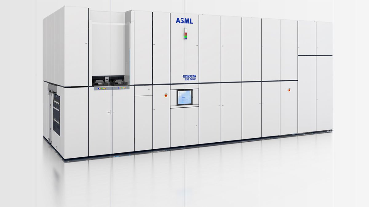
ASML sold 7 EUV machines in Q1, Intel bought ... none of them

But I guess we'll hear soon that: "7nm is on schedule and beating internal estimates"

I mean, Intel has all the EUV machines they need alright, right?!?!?
 

LP-ZX100C

Junior Member
Mar 16, 2021
10
17
41
I mean, Intel has all the EUV machines they need alright, right?!?!?

So , after all, it's inline what Charlie from Semiaccurate said in a call with Susquehanna about Intel buying tools also Intel doesn't believe in their own roadmaps, too.
 

Asterox

Golden Member
May 15, 2012
1,026
1,775
136
Last edited:

Hulk

Diamond Member
Oct 9, 1999
4,191
1,975
136
Is machine learning used when designing processors? Seems like it would be a great application. Basically tell the "machine" you have this many transistors and you need to run this code as fast as possible (from an IPC point of view), find the best way to to do it. Obviously that is greatly simplified but you know what I mean.
 

DrMrLordX

Lifer
Apr 27, 2000
21,582
10,785
136
Is machine learning used when designing processors? Seems like it would be a great application. Basically tell the "machine" you have this many transistors and you need to run this code as fast as possible (from an IPC point of view), find the best way to to do it. Obviously that is greatly simplified but you know what I mean.

Machines designing machines is still a ways off. We don't have The Architect quite yet.
 
  • Like
Reactions: Tlh97 and Hulk

moinmoin

Diamond Member
Jun 1, 2017
4,933
7,619
136
Is machine learning used when designing processors? Seems like it would be a great application. Basically tell the "machine" you have this many transistors and you need to run this code as fast as possible (from an IPC point of view), find the best way to to do it. Obviously that is greatly simplified but you know what I mean.
As @DrMrLordX said AI designing processors is far off. What's more and more automated is the layout on silicon. I think AWS referred to its Graviton ARM server chips as being optimized using AI.
 

mikk

Diamond Member
May 15, 2012
4,111
2,105
136
Q1 Earnings Call:

As a sign of our improving execution, we qualified Tiger Lake-H ahead of schedule in 10 nanometers, and we expect 10-nanometer unit volumes to cross over 14 nanometers in the second half of the year.


10nm ULV market volume is already higher than 14nm, Tigerlake-U is still growing while CML-U is declining more and more. On ADL/SPR/MTL:

In the PC business, we will follow the successful launches of Tiger Lake and Rocket Lake with Alder Lake, which is currently sampling and will ship in the second half of this year. Within the next couple of weeks, we’ll tape in the compute tile for Meteor Lake, our first 7-nanometer CPU for 2023. In the data center, we will follow the strong ramp of Ice Lake with Sapphire Rapids, which is scheduled to reach production around the end of this year, and ramp in the first half of 2022.
 

DrMrLordX

Lifer
Apr 27, 2000
21,582
10,785
136
Not sure if I agree with Dr. Cutress. Alder Lake-S with DDR4 is better than 3-6 months more of Rocket Lake-S.
 

tomatosummit

Member
Mar 21, 2019
184
177
116
I somewhat agree with him but it's more of a lesser evil thing and the market is different now compared to skylake launch. Haswell-E started off the consumer ddr4 market with it's own foibles but the enthusiast segment will more easily adopt a newer memory standard. Although I see mob manufacturers just releasing a variety of boards, ddr4 at the lower budget, rgb extreme ddr5 boards and some combos.
This is the year for everything being delayed though so the ddr5 ramp might be late and cause additional problems, especially as we have so little information on epyc4 and sapphire rapids and their launch windows.

Regarding his "20% IPC" statement, isn't that only people misreporting intel's own "20% more single thread performance" they haven't specified ipc themselves yet.
 

jpiniero

Lifer
Oct 1, 2010
14,509
5,159
136
I somewhat agree with him but it's more of a lesser evil thing and the market is different now compared to skylake launch. Haswell-E started off the consumer ddr4 market with it's own foibles but the enthusiast segment will more easily adopt a newer memory standard. Although I see mob manufacturers just releasing a variety of boards, ddr4 at the lower budget, rgb extreme ddr5 boards and some combos.

A combo board is asking too much, DDR5 is pretty different from DDR4. I don't see DDR5 being unavailable as being a problem as long as Alder Lake's DDR4 support isn't a big regression.
 

tomatosummit

Member
Mar 21, 2019
184
177
116
A combo board is asking too much, DDR5 is pretty different from DDR4.
Asrock will be taking that bet.
If ddr4+5 is the real reason for the extra 500pins on the socket then it would be trivial to add. Each dimm socket would be wired to unique pin sets on the socket, the only complications I see would be electrical interferance and convincing accounting.
 

Mopetar

Diamond Member
Jan 31, 2011
7,797
5,899
136
I had assumed that Zen 4 would using DDR5 so it make sense for Intel to also provide support for it. He does mention that it's a chicken and egg problem, but the surest way to get something made is by creating demand for a product.
 

eek2121

Platinum Member
Aug 2, 2005
2,904
3,906
136
I am sorry, this post has been a bit delayed, day job and all.

Yea I mean, if you look at Tigerlake, 15W barely serves 4 cores. AMD has 8 because not only it's smaller but more power efficient too.

The decisions are probably arbitrary as well. Marketing, profits, performance all play a role. 8+8+2 is possible too, but will it make sense as a brand, perf/watt, and in revenue terms?

Golden Cove, unless they change the design paradigm it's likely it won't be more efficient in MT. The growth in transistors don't result in corresponding increases in performance.

I won't bet on ESF being a big of a gain as SF. 10nm Icelake process sucked, so SF had lot more potential. SF brought 20% gains. ESF, maybe 7-10% on top of that?

For someone named IntelUser2000 you seem to be pessimistic regarding Intel. When Intel finalized TGL-U, 10nm was still an uncertainty and Renoir was not even announced or launched. More on this in a moment.

Is there some evidence DDR5 won't be ready this year? More and more news are coming about DDR5, recently from Micron/Crucial: https://wccftech.com/crucial-ready-mainstream-ddr5-memory-modules-sodimm-udimm-4800-mhz-32-gb/

DDR5 will likely launched in Q4. If ADL-S is DDR5 only at launch, it will likely launch in January...a year after rocket lake. We will probably see a server variant, and if we are lucky mobile, but I strongly suspect desktop to launch in January. I hope I am wrong. Believe it or not, I LOVE to be wrong.

Now, back to TGL-U, when TGL was being developed, 10nm had poor yields, 10SF had just completed testing, and the best AMD had was the Ryzen 3000 mobile chips. TGL-U, as it stands, would walk all over Ryzen at the time, Intel also strongly suspected that it would also walk all over Zen 2. They were right. The issue is that the U parts were designed around quad core parts. Intel did not focus on 8-core parts due to 10nm issues at the time.

When the chip launched, a bunch of people piled on and said that the flagship TGL-U chips used too much power because they briefly spiked very high. Anyone that argued TDP and power usage in the same sentence needs to go back and understand that TDP != power usage. Tiger Lake actually appears to obey "TDP" for the first time ever. That is, A TGL-U chip will burst super high, but quickly drop once TDP is met. There is no issue with a chip consuming even 200W of power as long as the 15W TDP is met (I feel like yelling at AMD, Intel, NVIDIA, shoot, anyone making "processors" for allowing this to ben open definition).

AMD originally designed Renoir around 6 cores with much higher clocks. They quickly discovered they could lower clocks, but increase core counts. That was their strategy.

If you compare a Ryzen 4800U with 4 cores disabled vs. a top of the line TGL-U chip, the TGL-U chip will win. If you compare Intel's offering to AMD's chip with only 6 cores disabled, the Intel offering will win in most cases/be neck in neck with the rest.

That is pretty much all I have to say. Now, before you begin your attack, I have a ton of hardware in my household, and you should know and understand that the only Intel CPU that exists is in an aging my spouse uses. I hold no Intel stock, and I held AMD stock for years on and off until tonight when I sold at $89. Please note that I will be buying back, but I know the market, and I know that the stuck will dump (it already has :D)

AMD has a fantastic product. However, TGL-H actually competes VERY well with Cezanne, (the 11800H beats the 5900HX in Geekbench, Cinebench, and a few other benchmarks that I'm privy to. Don't bother asking, the chip is dropping soon) and that is why I think Alder Lake will surprise us. If you actual evidence to the contrary I'd love to debate it, as it is likely something I've not seen. Until then, as I see leaks I will post them here. Love you all! :)

EDIT: My actual thoughts are: Alder Lake Desktop in January, Mobile in Q2, and workstation/server variants between the two. I think Alder Lake will have Xeon offering, but Sapphire Rapids/Ice Lake will rule the roost for high end. ADL-S will be mid-range to low end. I know not much has leaked out regard that, but IMO that is a sensible play.
 
  • Like
Reactions: lightmanek

zir_blazer

Golden Member
Jun 6, 2013
1,160
400
136
The only time that I recall AMD being on top of Intel adopting a new RAM type was with the original DDR and that is because Intel tried to force RamBus onto everyone, and failed catastrophically. All the other DDR generations the new DDRx was far more expensive at the same capacity levels and usually equal or just slighty below/above in performance because the speeds and Timmings were horrible. I don't see positive that AMD takes the first shot, maybe in Server (Like Intel with DDR4 and Haswell-E) if DDR5 allows for greater densities or using a dual controller like AM3 doing both DDR2 and DDR3 or even Intel Skylake supporting DDR3 and DDR4.
It makes sense to me that AMD is already prepared for such case where poor RAM adoption forces a new AM4 release, unless they want to upgrade the Socket anyways and have Motherboards with one of the two slots types. The question is whenever the IO dies already can do both modes or you need a new one.

And Alder Lake big.LITTLE... The horror. I'm expecting something worse than AMD CMT in Bulldozer, unless Intel is working VERY close to Microsoft to make sure than the CPU Scheduler will not wreck the party. For me it is a bad idea since implementing it properly seems far more complex than it looks. And cores not being equal means that possible behavior like erratas and bugs affects them in different ways. Imagine if a piece of code produces one result if executed in a big Core but another in the smaller Core. Harder to debug.
 

Hulk

Diamond Member
Oct 9, 1999
4,191
1,975
136
I thoroughly enjoyed watching Ian's entire 26 minute video, which is rare for me with a video that long. I have been thinking the same thing as Ian regarding the Golden Cove 20% IPC improvement that has been stated (I don't even remember the origin of this) and the Scheduler issues with Big/Little and how they will be handled. Namely, from an architectural level Intel has not told us, even in general terms, how it plans on improving IPC by 20% over Sunny Cove and how the heterogeneous cores will be effectively utilized by Windows?

The DDR4/5 issue I think is a little more out of Intel's hands. They are still quite the juggernaut in terms of sheer volume but perhaps not as able to "force" massive swings in the adoption of technology on their schedule.

It does kind of put them in a bind. If they wait on DDR5 because it is critical to Alder Lake performance vs Zen 3 then they remain behind Zen 3 while AMD sits back and quietly continues to ship Zen 3 while preparing for the release of Zen 4 when DDR5 is ready for widespread adoption. The current Rocket Lake vs. Zen 3 is not a great situation for Intel.

On the other hand is they put out Alder Lake predominantly with DDR4 (meaning that's how users will have to set it up due to lack of cost effective DDR5 memory) and performance suffers dramatically they they will get blasted by reviewers, may still be behind Zen 3, and will have this messy development of ADL as the shift to DDR5 occurs. By the time DDR5 is widespread Zen 4 will most likely be released and quite possibly providing AMD with a continuing performance/efficiency lead.

I'm thinking their best play here is to release ADL with DDR4/5 support and make sure review kits are DDR5. Assuming performance is impressive, if DDR4 performance isn't they have the caveat of simply ignoring DDR4 performance metrics, and we know Intel is good at making believe certain known facts don't exist, like the fact that the 5800X is a better performer than the 11900K while being cheaper and more power efficient.

Or, the old Intel may return and blow our minds in Core2Duo fashion circa 2006. Hopeful for that but I don't think it likely.