[Anandtech]: GlobalFoundries Stops All 7nm Development !!

Page 10 - Seeking answers? Join the AnandTech community: where nearly half-a-million members share solutions and discuss the latest tech.

zinfamous

No Lifer
Jul 12, 2006
110,562
29,171
146
AMD currently only uses Hynix for their HBM needs, right? I wonder if moving to Samsung at some time in the future and for a specific product line--some sort of low-to-mid range APU w/ HBM for specific OEM needs--makes a lot of sense?

Hynix only makes 4gb stacks of HBM2, right? I wonder if there is some design/efficiency advantage if they can work with an integrated single stack of 8gb HBM2 from Samsung. Is their some reason that Samsung nodes, which are primarily used for ARM-based chips, don't translate well for x86 architectures?
 

NostaSeronx

Diamond Member
Sep 18, 2011
3,686
1,221
136
New Gary Patton (CTO of GF) interview about the 7nm abandonment
Is it 7nm abandonment?
GF is realigning its leading-edge FinFET roadmap to serve the next wave of clients that will adopt the technology in the coming years. The company will shift development resources to make its 14/12nm FinFET platform more relevant to these clients, delivering a range of innovative IP and features including RF, embedded memory, low power and more. To support this transition, GF is putting its 7nm FinFET program on hold indefinitely and restructuring its research and development teams to support its enhanced portfolio initiatives. This will require a workforce reduction, however a significant number of top technologists will be redeployed on 14/12nm FinFET derivatives and other differentiated offerings.
Later on it states:
GF is intensifying investment in areas where it has clear differentiation and adds true value for clients, with an emphasis on delivering feature-rich offerings across its portfolio. This includes continued focus on its FDXTM platform...

A Special highlight regarding the "wunderWaffe" 12FX, certain people are pushing non-stop as the "new 7nm":
It largely depends on the 22FDX+ node. 12FDX is an improvement upon 22FDX+ not 22FDX.
https://i.imgur.com/KOYu5AD.png <== STMicroelectronics roadmap
// The project objectives have been precised in the technical annex of the amendment submitted in September 2016. WAYTOGO FAST targeted products aims to open a sustainable route to FDSOI technology by extending the scope of the 28nm node and supporting the 22/22+ nm nodes.
https://cordis.europa.eu/result/rcn/196500_en.html
https://www.electronicsweekly.com/news/business/nano16-fd-soi-moves-towards-22nm-2016-11/

The most likely case is that 12FDX was delayed for 10FDSOI/7FDSOI options. While STM's 28FD and GF's 22FD implement things meant for 14FD/14FD+/12FDX. Hence, the 22FD+ node, but STMicroelectronics has halted 28FD in support of GloFo: https://www.st.com/content/st_com/en/about/media-center/press-item.html/t4012.html
This reduces fragmentation with CEA Tech, so they don't have to support two node roadmaps. As implied in the CEA Leti annual report 2016: "After the STMicroelectronics collaboration on 28nm FDSOI (and on 14nmFDSOI, 14+FDSOI), LETI experts have engaged with Global Foundries (GF) to support the development (in Malta , US) and industrialization (in Dresden, Germany) of 22FDX. In addition, Leti continues to explore new techniques and modules to help the IC makers to shape the next technology nodes (12FDX for GF, 28FDSOI ULP for STM)."
Back to the Waytogofast:
"Performance boosters developed for the 14FDSOI and the 14FD+ have started to be reengineered to be applied to the 28FDSOI Derivatives : the gate stack change : from HfSiON to HfO2, the dual workfunction gate metals, the SiGe channel for the PMOS, the Low k spacers integration."

Learn on 22FDX+, improve on 12FDX.

22FDX+ only needs to beat 22HPC+/22ULP from TSMC and 22FFL from Intel. The improvements set forth could easily push 22FDX+ ahead in drive current. Which would solidify 22FDX+ as the big die of that bunch. 12FDX being delayed and utilizing improved 22FDX+ and forward 10FD/7FD perf boosts. Would most definitely be on-par or ahead with 10nm/7nm FinFET drive currents.

On the Samsung side after 18FDS:
-> Internal research rather than CEA-Leti.
-> GlobalWafers SOI focus rather than SOITEC.
-> Less aggressive on performance. (FinFETs > FDSOI)
"GlobalWafers will see a meaningful expansion of its production capabilities and breadth in product and global customer base, including greater access to the Korea and EU as well as SOI product technologies and capacity."
From GlobalWafers Successfully Consummates Acquisition of SunEdison Semiconductor

Which will now contrast against GlobalFoundries which will be (FDSOI > FinFETs).
 
Last edited:
  • Like
Reactions: amd6502

Ajay

Lifer
Jan 8, 2001
15,429
7,847
136
As far as volume constraints, I bet TSMC will give AMD more volume than GF could ever supply.
At first I was skeptical, but TSMC does seem to be able to ramp up FABs pretty quickly, as they did for Apple. AMD seems to be willing to pay the extra cost of risk production to get it's 7nm Vega product out on time, so all seems to be well ATM. That said, this will be an interesting transition to watch; it's not like TSMC is infallible or that AMD has the deep pockets that Apple has.
 

PeterScott

Platinum Member
Jul 7, 2017
2,605
1,540
136
AMD currently only uses Hynix for their HBM needs, right? I wonder if moving to Samsung at some time in the future and for a specific product line--some sort of low-to-mid range APU w/ HBM for specific OEM needs--makes a lot of sense?

Hynix only makes 4gb stacks of HBM2, right? I wonder if there is some design/efficiency advantage if they can work with an integrated single stack of 8gb HBM2 from Samsung. Is their some reason that Samsung nodes, which are primarily used for ARM-based chips, don't translate well for x86 architectures?

Who you buy your RAM from has nothing to do with who you use as a foundry for your own parts.
 

amd6502

Senior member
Apr 21, 2017
971
360
136
Is it 7nm abandonment?

Later on it states:


It largely depends on the 22FDX+ node. 12FDX is an improvement upon 22FDX+ not 22FDX.
https://i.imgur.com/KOYu5AD.png <== STMicroelectronics roadmap

[....]

Learn on 22FDX+, improve on 12FDX.

12LP will be the benchmark to beat for mainstream chips. The designs are there, it's cheap, and it performs well. A few years out it maybe people won't consider it to perform well enough; given that 7nm is so expensive and impractical, your idea of 12FDX as successor seems to make much sense.

Do you think the manufacturing price/perf advantage of FDSOI would make it worth trying to adapt Zen2 to 12FDX (or redesigning it as a successor Zen3 for 12FDX).

This move to FDSOI will be interesting to watch. You mentioned

https://www.oracle.com/servers/sparc/m7-8/index.html

what are some other interesting (big cores or big GPU) products coming out on 22FDX (or related)?
 

USER8000

Golden Member
Jun 23, 2012
1,542
780
136
AMD currently only uses Hynix for their HBM needs, right? I wonder if moving to Samsung at some time in the future and for a specific product line--some sort of low-to-mid range APU w/ HBM for specific OEM needs--makes a lot of sense?

Hynix only makes 4gb stacks of HBM2, right? I wonder if there is some design/efficiency advantage if they can work with an integrated single stack of 8gb HBM2 from Samsung. Is their some reason that Samsung nodes, which are primarily used for ARM-based chips, don't translate well for x86 architectures?

You got it the wrong way around. AMD was scheduled to use Hynix,but they delayed production by over a year,so they ended up with slower Samsung HBM2. Now,Hynix is making faster HBM2,AMD is using it:

https://www.anandtech.com/show/13210/amd-announces-radeon-pro-wx-8200
 

NostaSeronx

Diamond Member
Sep 18, 2011
3,686
1,221
136
what are some other interesting (big cores or big GPU) products coming out on 22FDX (or related)?
Oracle M8+ which is the last Oracle chip since M9 was cancelled. Which is launching between 11.5 and 11.6 Solaris 11.next.
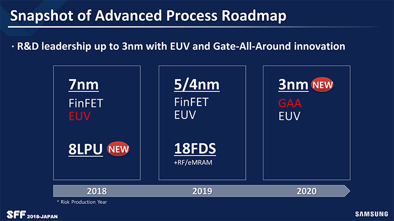
- Either from Samsung's S1 or S2 Fab for 18FDS(Plus?) or GlobalFoundries 12FDX @ Fab 1 or Fab 8.
// Oracle around ~2014 was aware of FinFET vs FDSOI. At the time they were looking at SOI FinFETs over Bulk FinFETs, so 14HP/14HP+ could also be M8+. Unless, they are following IBM to UTBB FDSOI. Which since, they never went FinFET and stayed Planar, the only choice is 12FDX. As 12FDX has a shrink in CPP/track height and a shrink in Mx compared to 20SoC/20HP @ TSMC.

IBM POWER9+/z14+ will most likely use a 14HP+ design which will support MRAM/ReRAM/etc. POWER10 and next-gen Z will be re-architected from "10HP" to 12FDX or 7FDX.

AMD's Excavator and Jaguar depending on whats cheapest to be the successor to Stoney Ridge. There is also Oland with the Small Vega, Cape Verde -> Polaris 12 -> Vega 12. Oland went Iceland, but nothing after that. So, that is prime for 22FDX/22FDX+.
Stoney Ridge -> "Blank" in the Ax/Fx continutation series. // 22FDX -> 12FDX
Iceland/Topaz -> Vega 16?/Navi 16? sub-RX 640 // 22FDX -> 12FDX
Generally speaking dGPU would be sub-100 mm squared and APU would be sub-125 mm squared. So, it could get the 22FDX LP treatment at any time.

Rockchip OP2 and OP2 Pro could be 22FDX with Cortex A76 + Cortex A55.

HiSilicon has an empty space for Kirin 94x for 22FDX. Which most likely be purely Cortex A55. Not really big core or anything.

MediaTek's Helio P18; MT6755S successor could also be 22FDX. With Helio P22/P60 both having a successor in 12FDX.

//Requirement is 22FDX+ gets near 22-nm HP ETSOI in drive current via other means than in the 22ETSOI strains of 2012. For 12FDX to match well in the high performance area. No FinFETs pretty much push investment towards this.

GlobalFoundries if going down the FDX path need to do more than just 22HP perf as well.
1. Malta needs to start 22FDX soon. Dresden needs to port RF 22FDX to Singapore.
2. After Chengdu starts, Dresden/Malta need to expedite 12FDX. Once the ramp is finish GloFo will want to port 12FDX to Chengdu(1st) and Singapore(2nd).

Getting all 300mm fabs to 22FDX and later 12FDX will be a revenue resource that will allow them to GigaFab all of them. >100,000 per month at four foundries will put it on-par with TSMC.

In regards, to big dies with AMD. FDSOI's architecture will be derived from both Excavator and Jaguar. 22FDX => XV/JG fusion, 12FDX => XV/ZN fusion, 7FDX => XV/ZN2-ZN4 fusion, 5FDXor3FDX => XV/ZN5 fusion. AMD has been avoiding extremely big dies like they did in the 2000s and Orochi(315 mm2 8-core)/Viperfish(>356 mm2 10-core). With Zen 8-core being 210 mm2, etc. So, big MCM and small chips are well within AMD's profile.

//also, can someone with better Chinese than that of web translation software translate:
https://www.globalfoundries.com/cn/...-chong-dian-guan-zhu-ri-yi-zeng-chang-de-chai
"格芯中国区总经理白农评论道,“对我们中国的客户及生产合作伙伴而言这是一个积极的变化,因为我们强化了聚焦差异化的技术比如FDX (FD-SOI)及其他。这些差异化技术在中国市场的需求不断增加,对格芯而言一直相当重要。我们对FD-SOI以及与成都政府合作的承诺从未改变。"

As it's not in the english version:
https://www.globalfoundries.com/new...n-growing-demand-for-differentiated-offerings
 
Last edited:
  • Like
Reactions: amd6502

DrMrLordX

Lifer
Apr 27, 2000
21,617
10,824
136
POWER10 and next-gen Z will be re-architected from "10HP" to 12FDX or 7FDX.

No! Power10 has a 2020 launch window. GF is only just now getting play from 22FDX. Do you honestly think anyone here is gullible enough to believe that a). GF is going to plow ahead with 12FDX research AND b). they'll have it ready by 2020?

No!

Also, GF has repeatedly stated that FDX nodes are not good for large ICs with heavy wire capacitance. IBM wants to quadruple their transistor count for POWER11 on 7nm versus Power8+. They are not going to switch to a Zen-like design featuring CCXs or anything else strung together by an interconnect like IF or Intel's mesh + EMIB future strategy. Intercore/interprocess latency is too important to their designs. Expect large dice for POWER10 and POWER11, or nothing at all.

IBM is either going to dump a mountain of cash on GF to get them to finish the custom, unnamed 10nm process, or they will call it quits on their old engineer teams/fabs and move production elsewhere. Every POWER design since at least POWER8 has been on a custom, expensive "boutique" node that presumably took a lot of up-front investment and that was used by practically nobody else. It's part of what you pay for when you get a POWER system.

AMD's Excavator and Jaguar depending on whats cheapest to be the successor to Stoney Ridge.

Neither Con cores nor cat cores show up anywhere on AMD's future roadmaps. No!
 

amd6502

Senior member
Apr 21, 2017
971
360
136
IBM is either going to dump a mountain of cash on GF to get them to finish the custom, unnamed 10nm process, or they will call it quits on their old engineer teams/fabs and move production elsewhere. Every POWER design since at least POWER8 has been on a custom, expensive "boutique" node that presumably took a lot of up-front investment and that was used by practically nobody else. It's part of what you pay for when you get a POWER system.

Nosta: "IBM POWER9+/z14+ will most likely use a 14HP+ design which will support MRAM/ReRAM/etc. POWER10 and next-gen Z will be re-architected from "10HP" to 12FDX or 7FDX."

Good point about IBM.

Power 8 (22nm SOI) and Power 9 (14nm fin FET) are all large dies, and Z14 looks to be even bigger. https://en.wikipedia.org/wiki/Category:IBM_microprocessors These all being high margin products would make higher cost of 7nm not be a huge issue. Hopefully they will have little trouble with availability and moving from GF to Samsung or TSMC. Or with GF screwing them so badly they may even collaborate with Intel (Isn't Jim Keller helping there now with 10nm foundry issues?).

Nosta is talking about Power10 successor, so this is a few years out, even one to a few years out from 2020. By then they may have addressed such limitations.

Neither Con cores nor cat cores show up anywhere on AMD's future roadmaps. No!

But it would make a lot more sense for mass consumer items like lo to mid range APUs. They don't show up on the roadmaps YET. True, but would it make sense sometimes to surprise? or even to adapt to changes in the environment, like the known reality about GF temporarily giving up on 7nm. I think XV+Jaguar merge could achieve excellent outcomes. You get a 4 thread CCX that would have excellent power consumption at lower frequencies, and excellent performance at mobile wattages. The benchmarks (price/perf and total performance) to beat would be against GF made 12nm Picasso-L 2c/4t which (assuming there is a L-variant) we expect very soon now.
 
Last edited:

Obvcop

Junior Member
Mar 7, 2017
11
12
36
No! Power10 has a 2020 launch window. GF is only just now getting play from 22FDX. Do you honestly think anyone here is gullible enough to believe that a). GF is going to plow ahead with 12FDX research AND b). they'll have it ready by 2020?

No!

Also, GF has repeatedly stated that FDX nodes are not good for large ICs with heavy wire capacitance. IBM wants to quadruple their transistor count for POWER11 on 7nm versus Power8+. They are not going to switch to a Zen-like design featuring CCXs or anything else strung together by an interconnect like IF or Intel's mesh + EMIB future strategy. Intercore/interprocess latency is too important to their designs. Expect large dice for POWER10 and POWER11, or nothing at all.

IBM is either going to dump a mountain of cash on GF to get them to finish the custom, unnamed 10nm process, or they will call it quits on their old engineer teams/fabs and move production elsewhere. Every POWER design since at least POWER8 has been on a custom, expensive "boutique" node that presumably took a lot of up-front investment and that was used by practically nobody else. It's part of what you pay for when you get a POWER system.


Neither Con cores nor cat cores show up anywhere on AMD's future roadmaps. No!
Where does this dude get this nonsense from, are we seriously expected to believe glofo cancelled all bleeding edge nodes and Amd shifted their entire future ryzen and gpu stack to tsmc. YET AMD are somehow going to port zen2 to 12fdx (which we don't even know for sure is coming out), develop and release a new bulldozer then beats ryzen, and then on top of that we are somehow to believe that glofo are secretly developing a 7nm soi node as well? Seriously, like how are these blatant lies and half rumours allowed on a forum like this At least with wccftech they are upfront about a rumour mill but nostro seems to just pull information out of nothing and declare it to be true
 

NostaSeronx

Diamond Member
Sep 18, 2011
3,686
1,221
136
@DrMrLordX
Will 12FDX be ready by 2020. Yes!
12FDX was delayed because of customers going on to 22FDX first.

GlobalFoundries has not said FDSOI has bad wire capacitance issues or bad drive current.
-> Gary Patton: I am a big fan of finFETs. I spend a lot of my time on 7nm.
Which makes him an unreliable source currently. The work and lifeblood of the CTO was cancelled. It seems pretty much known to him since May 2018. So, it comes off very edgy coming from him when he says "FDSOI doesn't compete."

Then, you have this:
"Outstanding 12FDX Customer Support: Technology and PPA Analysis for Major Customers"
Which implies AMD and IBM choose 12FDX. Since, AMD is the largest customer and IBM is the most expensive. Why would it be outstanding if they didn't get AMD and IBM?
As far as I am considered that was with PDK v0.1!

GlobalFoundries "realigning" FinFETs opens up FDSOI's later perf boosts to be pulled up.
Which starts with 22FDX+ w/ 2H2018/1H2018

@Obvcop
I'm talking about this 7nm FDSOI
Leti_Tokyo_FDSOI_roadmap_slide16.jpg

https://i1.wp.com/soiconsortium.eu/wp-content/uploads/2017/08/Leti_Tokyo_FDSOI_roadmap_slide16.jpg

Reposting STM/GF roadmap:
https://i.imgur.com/KOYu5AD.png

GlobalFoundries is a bit asymetrical on 22FDX/12FDX:
https://www.semiwiki.com/forum/content/5301-iedm-blogs-part-3-global-foundries-22fdx-briefing.html
"The front-end-of-line (FEOL) transistor is licensed from ST Micro’s 14nm FDSOI process."

22FDX+ uses 14FD+
12FDX would then use 10FD rather than 14FD+.
7FDX would be symmetrical and be that 7nm FDSOI node with the 7nm BEOL of 7LP.

https://pbs.twimg.com/media/DEsH3qiXcAADlLR.jpg
7FD is actually 10FD+, btw.
 
Last edited:

Gideon

Golden Member
Nov 27, 2007
1,619
3,645
136
@DrMrLordX
Will 12FDX be ready by 2020. Yes!
12FDX was delayed because of customers going on to 22FDX first.
Ok, bookmarked tagged and bagged. Wasn't the Carrizo's successor supposed to on 22FDSOI by your claims (I think Carrizo itself even) like in 2015-2016? I shall anxiously await till 2019-2020 to see progress on those huge chips from IBM and AMD coming out on 12FDX by 2020 ;)

And unless ATIC manages to sell GloFo, i'm more than sceptical about 10nm and 7nm SOI as well.
 

NTMBK

Lifer
Nov 14, 2011
10,232
5,012
136
But it would make a lot more sense for mass consumer items like lo to mid range APUs. They don't show up on the roadmaps YET. True, but would it make sense sometimes to surprise? or even to adapt to changes in the environment, like the known reality about GF temporarily giving up on 7nm. I think XV+Jaguar merge could achieve excellent outcomes. You get a 4 thread CCX that would have excellent power consumption at lower frequencies, and excellent performance at mobile wattages. The benchmarks (price/perf and total performance) to beat would be against GF made 12nm Picasso-L 2c/4t which (assuming there is a L-variant) we expect very soon now.

But that theoretical Excavator derived core would still give you lower single threaded performance than a two-core Zen CCX. While also being significantly more expensive to develop (being essentially a whole new architecture), at a time when AMD should be focusing its resources on a) Zen 2/Zen 3 roadmap and b) fixing their GPU business, and winning next gen consoles.
 

NostaSeronx

Diamond Member
Sep 18, 2011
3,686
1,221
136
Ok, bookmarked tagged and bagged. Wasn't the Carrizo's successor supposed to on 22FDSOI by your claims (I think Carrizo itself even) like in 2015-2016? I shall anxiously await till 2019-2020 to see progress on those huge chips from IBM and AMD coming out on 12FDX by 2020 ;)
So, AMD was the one that made GlobalFoundries go "Advanced FDSOI" and adopt "14LPP" from Samsung.

Skybridge went from Nolan/Amur to Zen/K12. (K12 got dropped)
20LPM(XV)/14XM(Post-15h) went Advanced FDSOI and 12nm FDX with post-15h only.
The individuals who built Stoney Ridge are/were slotted for Advanced FDSOI/22FDX. With the undisclosed x86 core, that would replace 15h with higher single threaded performance and being less expensive to develop. It's roadmap follows Nolan, but goes down rather than up. Perf/watt is more power efficiency than performance like Zen.

Carrizo was 28nm FDSOI. That was canned for 28A and later 28HPA. 20LPM cancelled, 28FDSOI cancelled, whelp GF28A time. AMD also explored 28nm from UMC, that was quickly shot down.
De74XY1.png

https://i.imgur.com/De74XY1.png
This pre-7LP comparison: https://images.anandtech.com/doci/13171/15335754089771237328638.jpg
10FF => 7FF is a >20% increase in perf however. While 12FDX in early 2019 costs less than 28nm LPS.
And unless ATIC manages to sell GloFo, i'm more than sceptical about 10nm and 7nm SOI as well.
ATIC? Who is that?

I'm joking but here:
"Launched in 2009 through a partnership between Advanced Technology Investment Company (ATIC), which is now Mubadala’s Technology unit, and Advanced Micro Devices (AMD)."

2017 => Mubadala Technology gave Dresden/Fab 1 ~1.75 billion USD for that 40% increase in 22FDX.
// https://www.anandtech.com/show/11117/globalfoundries-to-expand-capacities-build-a-fab-in-china
So, they might sell Malta? That is unlikely as it can be repurposed for 22FDX and 12FDX.
 
Last edited:

french toast

Senior member
Feb 22, 2017
988
825
136
If TSMC can guarantee AMD all the capacity it needs, not just at current production.. but room to expand and grow..then yes I can see AMD staying at TSMC for the foreseeable future..but I maintain that AMD will look to dual source at some point in future, it is a strategy that has worked when glofo let the side down.
If the Q4 product tape out that was moved or cancelled was for a 7nm APU next year, and TSMC didn't have the required capacity, then I don't see why AMD couldn't tap up Samsung for their 8nm LPP process, after all an APU doesn't need high clocks..

Then stay at Samsung fabbing APUs on their advanced LP nodes, maybe even move consoles over there?.
 

PeterScott

Platinum Member
Jul 7, 2017
2,605
1,540
136
If TSMC can guarantee AMD all the capacity it needs, not just at current production.. but room to expand and grow..then yes I can see AMD staying at TSMC for the foreseeable future..but I maintain that AMD will look to dual source at some point in future, it is a strategy that has worked when glofo let the side down.

Someday they might dual source to Samsung, or who knows, Intel will straighten out their own 7nm and they will Fab at Intel, or GF will reveal that secret 7FDX process and take over the world. ;)

But it none of these are likely anytime soon. Samsung is even being skipped by long time partners like Qualcomm, who likely have good visibility on how late 7nm is going to be at Samsung. Just like AMD was aware how late GF was going to be, and had most of it's designs at TSMC already.

It looks like AMD had very little confidence in GF 7nm, so whatever they were considering taping out there first was either:
a) Dual sourced with TSMC already:
b) Low importance pipe cleaner part.

Thus I have ZERO concern GF throwing in the towel on leading edge, will have any negative impact on AMD. I only see it as a positive. It removes millstone from AMDs neck for new products.
 

french toast

Senior member
Feb 22, 2017
988
825
136
Someday they might dual source to Samsung, or who knows, Intel will straighten out their own 7nm and they will Fab at Intel, or GF will reveal that secret 7FDX process and take over the world. ;)

But it none of these are likely anytime soon. Samsung is even being skipped by long time partners like Qualcomm, who likely have good visibility on how late 7nm is going to be at Samsung. Just like AMD was aware how late GF was going to be, and had most of it's designs at TSMC already.

It looks like AMD had very little confidence in GF 7nm, so whatever they were considering taping out there first was either:
a) Dual sourced with TSMC already:
b) Low importance pipe cleaner part.

Thus I have ZERO concern GF throwing in the towel on leading edge, will have any negative impact on AMD. I only see it as a positive. It removes millstone from AMDs neck for new products.
We agree on something then, AMD will be better off without GF, I think Qualcomm moving to TSMC has more to do with Samsung 7nm being much later than TSMC, even though it looks like Samsung 7nm might be more advanced, Qualcomm probably looked at performance difference between Samsung's available process (8nmLPP) and a early TSMC 7nm..and decided TSMC is best for them...fair play.

Could be that all advanced 7nm LPE EUV is reserved for Exynos, with not enough capacity for Qualcomm needs, or price difference.

Like I said, TSMC has very good process, if they have sufficient capacity for AMD needs, then they will be happy with TSMC..for now.
I don't see how moving the right chips over to Samsung could be bad in future, they have leading edge low power processes and loads of capacity that needs filling..meaning AMD can barter a good deal.

GPU and Desktop could be served by TSMC.
APU,Server and consoles? Could be done at Samsung.
Just my thoughts.
 
  • Like
Reactions: Lodix

PeterScott

Platinum Member
Jul 7, 2017
2,605
1,540
136
GPU and Desktop could be served by TSMC.
APU,Server and consoles? Could be done at Samsung.
Just my thoughts.

Again maybe, someday, when Samsung has a mature trustworthy process. Who knows. It's all TSMC for leading edge for the immediate future.

On consoles. Does AMD actually deal with Fabbing those? I was under the impression AMD works with console makers to design the chips and then charges them royalties on the design, but isn't really involved in Fabbing. Does anyone know?

I looks like the NVidia console deals were Royalty deals:
https://www.nvidia.com/object/IO_17342.html

And Microsoft was already using TSMC as Fab for Xbox APUs
https://en.wikichip.org/wiki/microsoft/scorpio_engine
 
  • Like
Reactions: french toast

naukkis

Senior member
Jun 5, 2002
705
576
136
On consoles. Does AMD actually deal with Fabbing those? I was under the impression AMD works with console makers to design the chips and then charges them royalties on the design, but isn't really involved in Fabbing. Does anyone know?

AMD can't licence x86 to third parties. So it's AMD fabbed and sold parts.
 

DrMrLordX

Lifer
Apr 27, 2000
21,617
10,824
136
Nosta is talking about Power10 successor, so this is a few years out, even one to a few years out from 2020. By then they may have addressed such limitations.

I don't think GF will ever address the limitations of their FDX nodes. Wire capacitance doesn't just go away. IBM is not looking to run small dice, either.

But it would make a lot more sense for mass consumer items like lo to mid range APUs.

Not really. Zen 1 on 14LPP has already shown that it actually scales downward in clock/voltage really well. A single-CCX Zen 1 on a 7nm node would be tiny, sip power, and easily maintain clocks of 2 GHz or higher while sipping power. There's no need for AMD to keep burning money on Con core/cat core projects when the product they've had since 2017 will fit the bill very nicely. And that's not taking Zen+/Zen2 into account, either.

There is no known reason for them to go back to Con cores outside of . . . a certain user's obsession with them. And the cat cores? They were good for their time, sort of, but Nolan/Amur were both busts, and AMD has abandoned the tablet sector anyway. They are focusing on the server world first, HEDT/desktop second. Su doesn't seem interested in throwing a lot of money at low-end, low margin sales.

Where does this dude get this nonsense from, are we seriously expected to believe glofo cancelled all bleeding edge nodes and Amd shifted their entire future ryzen and gpu stack to tsmc. YET AMD are somehow going to port zen2 to 12fdx (which we don't even know for sure is coming out), develop and release a new bulldozer then beats ryzen, and then on top of that we are somehow to believe that glofo are secretly developing a 7nm soi node as well? Seriously, like how are these blatant lies and half rumours allowed on a forum like this At least with wccftech they are upfront about a rumour mill but nostro seems to just pull information out of nothing and declare it to be true

Usually as long as he stays out of the big threads, it's not a problem.

Will 12FDX be ready by 2020. Yes!

Assuming they even bother with 12FDX (which all their press releases seem to indicate is not the case), pushing out a few test SRAM cells by Dec 2020 hardly counts as availability; furthermore, it's highly probable that any future SOI nodes will be used for small signal processors, modems, and the like - not SoCs/CPUs or GPUs. It'll hardly be relevant, certainly not to IBM.

GF is signaling that they want to make a lot of sales on 14LPP, 12nm, and 22FDX. They don't want to throw a lot of cash at new nodes, period. The only question mark is IBM and what they're willing/able to do for them. But I see any FDX node as being a poor fit for current and future iterations of POWER.
 

NostaSeronx

Diamond Member
Sep 18, 2011
3,686
1,221
136
Thus I have ZERO concern GF throwing in the towel on leading edge, will have any negative impact on AMD.
*ahem*
https://i.imgur.com/fWbDoyZ.png
What is under "leading edge" and first in leading edge?
https://i.imgur.com/iTsYTT6.png
What is after 14nm but before 7nm?
https://i.imgur.com/az67Bar.png
If delayed and improved what node will the above node perform at if it was already near-equal to blank?
Assuming they even bother with 12FDX (which all their press releases seem to indicate is not the case), pushing out a few test SRAM cells by Dec 2020 hardly counts as availability; furthermore, it's highly probable that any future SOI nodes will be used for small signal processors, modems, and the like - not SoCs/CPUs or GPUs..
It's in a password lock zone now.
Old 12FDX already hit >70% LDY for SRAMs in 2017? With nFET being 98% ready for production and pFET being 90?% ready for production. It was set to be between the 7LP and 7LP EUV, btw.
The only question mark is IBM and what they're willing/able to do for them. But I see any FDX node as being a poor fit for current and future iterations of POWER.
IBM is going 12FDX and they want a second source. GlobalFoundries needs to provide two fabs for 12FDX, or IBM will pay them to give 12FDX to someone else.

Everything funnels into 12FDX.
28nm global ~1000 (by 2025)
22nm (FDSOI) global >1000 (by 2025)
14nm (FinFET w/ 12nm FF) global ~300 (by 2019) and ~400 (by 2025)
12nm (FDSOI) global >1000 (by 2025)
7nm is the oddity, but GlobalFoundries was set to only get >100 by 2021.
GlobalFoundries expectation is FinFETs make zero and FDSOI makes anything but zero. With FDSOI increasing wafer CAGR by >50% over current 28nm sales by 2025.

FinFETs => decreases wafers sold at GlobalFoundries
FDSOI => increases wafers sold at GlobalFoundries

So, the gloves are off at GlobalFoundries. FDSOI is getting the aggregate money slush from 7nm to 3nm. Of the $15 to >$20 billion that is now going into;
- UTBB Quantum
- UTBB RF
- UTBB High Performance
- UTBB Low Power
- UTBB Bipolar
- UTBB Analog and Power (IC VRM, IC DACs, etc)
Which all will start in 22FDX/22FDX+ before moving to 12FDX. Which will fuse HP 22FDX(HP/Q/Bi) and LP 22FDX(RF/A/P) into a single aggregate option: just 12FDX and HP/LP/Q/RF/Bi/A/P options. No split like 22FDX+ and 22FDX.
 
Last edited:

NostaSeronx

Diamond Member
Sep 18, 2011
3,686
1,221
136
Leading Edge is not over at GlobalFoundries.
Only FinFETs, IBM is aware of this decision and so was AMD. This list includes Qualcomm, MediaTek, HiSilicon, and Unisoc.

Everyone knew about GlobalFoundries cancelling FinFETs to improve upon FDSOI. The reasoning was simple, it had a higher return of investment for everyone. All of them wanted 12FDX over 7LP.

Once the restructuring from FinFETs and FDSOI to just FDSOI. GlobalFoundries will do some interesting things in Q1 2019.
---
"The only meaningful benefit of SOI for 14nm FF was to add eDRAM. Ironically that node is the first and last FF on SOI node of entire world. For the next nodes there is no choice for them other than using a foundry process (say 7nm at SS or TSMC) and drop eDRAM."
- Ali Khakifirooz, NVM engineer @ Intel, and one of the creators of UTBB FDSOI

and
7.png

3nm by 2020.

Do you think GlobalFoundries could have done this? (imho, no.)

IBM POWER roadmap doesn't not declare POWER10's node either.
https://pbs.twimg.com/media/DlKexFpX4AALa6B.jpg:large

eDRAM always fell way to eMRAM anyway:
https://pc.watch.impress.co.jp/img/pcw/docs/471/308/photo027.jpg
 
Last edited: