-
We’re currently investigating an issue related to the forum theme and styling that is impacting page layout and visual formatting. The problem has been identified, and we are actively working on a resolution. There is no impact to user data or functionality, this is strictly a front-end display issue. We’ll post an update once the fix has been deployed. Thanks for your patience while we get this sorted.
You are using an out of date browser. It may not display this or other websites correctly.
You should upgrade or use an alternative browser.
You should upgrade or use an alternative browser.
Discussion AMD's Soundwave ARM APU: The Beginning of Transformation !!!
Page 25 - Seeking answers? Join the AnandTech community: where nearly half-a-million members share solutions and discuss the latest tech.
Are you talking about that guy that said that AMD would be destroyed by ARM from below and Intel from above?
All in all, you remind me of someone from beyond3d forums (was it juanrga?).
Never listening to facts presented by others, always spinning your own tale, no matter how little sense it makes.
NTMBK
Lifer
Just wait until you find his alternative physics textbooks, ooh boy!!!!!!!!
Internet Strongman reference sighted! Batton down the hatches! Sound the alarms! We are not prepared for an incursion by Internet Strongman juangra!
igor_kavinski
Lifer
Made in Russia?Just wait until you find his alternative physics textbooks, ooh boy
NTMBK
Lifer
Because Juan is such a famous, quintessentially Russian nameMade in Russia?
Schmide
Diamond Member
This is the best of juanrga tech, he's from Spain btw.
https://www.juanrga.com/2018/10/basic-remarks-on-parallel-computing.html
Not the best intuition on computing, but good at presenting his arguments.
https://www.juanrga.com/2018/10/basic-remarks-on-parallel-computing.html
Not the best intuition on computing, but good at presenting his arguments.
DrMrLordX
Lifer
Just wait until you find his alternative physics textbooks, ooh boy
I don't think I can handle that.
marees
Platinum Member
poke01
Diamond Member
Why is it so big
marees
Platinum Member
Google AI overview scolds me (gaslights me?) & says no such socket as FF5 exists
- Mobile socket names: AMD has used many mobile BGA sockets over the years. Recent BGA platforms include:
- FP5: Used by early mobile Ryzen 7 and other processors in the Ryzen 7000 series, like the Ryzen 7 2700U.
- FL1: Used by high-performance mobile parts, including the Ryzen 9 7945HX3D.
- FP7/FP7r2: Used for Ryzen 7000 and earlier series mobile processors.
- Strix Point/Strix Halo: The latest series of mobile processors use BGA sockets and are often cited by their codenames.
marees
Platinum Member
Never mindGoogle AI overview scolds me (gaslights me?) & says no such socket as FF5 exists
- Mobile socket names:AMD has used many mobile BGA sockets over the years. Recent BGA platforms include:
- FP5: Used by early mobile Ryzen 7 and other processors in the Ryzen 7000 series, like the Ryzen 7 2700U.
- FL1: Used by high-performance mobile parts, including the Ryzen 9 7945HX3D.
- FP7/FP7r2: Used for Ryzen 7000 and earlier series mobile processors.
- Strix Point/Strix Halo: The latest series of mobile processors use BGA sockets and are often cited by their codenames.

Leaks Suggest AMD AM5 Future Support for Ryzen 9000G "Gorgon Point" & EPYC 4005 "Grado" CPUs
PC hardware watchers continue to pore over official AMD repositories and adjacent databases, in the hopes of finding unannounced next-gen technologies. Olrak29 and InstLatX64 have presented their latest Team Red-related findings; apparently reaching across futuristic desktop, mobile, and...
marees
Platinum Member
More confirmation from Google searchNever mind

Leaks Suggest AMD AM5 Future Support for Ryzen 9000G "Gorgon Point" & EPYC 4005 "Grado" CPUs
PC hardware watchers continue to pore over official AMD repositories and adjacent databases, in the hopes of finding unannounced next-gen technologies. Olrak29 and InstLatX64 have presented their latest Team Red-related findings; apparently reaching across futuristic desktop, mobile, and...www.techpowerup.com
Using the never-before-seen FF5 socket, AMD is also allegedly working on a new lineup of mobile offerings dubbed Soundwave. The rumor mill positions this as a low-power, Arm-based device from AMD, employing Radeon graphics. This might be AMD's response to Nvidia's rumored N1X SoCs for the WoA (Windows on Arm) ecosystem. If these SoCs are anywhere near their launch, we'll probably hear more about them at Computex.

AMD is reportedly readying Ryzen 9000G (Gorgon Point) and EPYC 4005 (Grado) CPUs for AM5
Along with several new Ryzen mobile offerings.
adroc_thurston
Diamond Member
yeah same swimlane as Van Gogh (that one was FF3 iirc).Using the never-before-seen FF5 socket
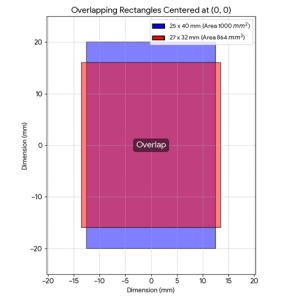
I have asked Gemini to overlap FF5 and STX FP8: Soundwave total package is about 86.4% of STX: most likely due to better power efficiency (STX has to draw up to 54W to support turbo boost). And please check the table I created in the frontpage. As I said, Soundwave is the successor of STX to compete with Apple M5 and Qualcomm's X2. So please don't believe in non-sense specs of 2P+4e and 4 RDNA3.5 CU with improved ML from MLID...
Last edited:
NTMBK
Lifer
The socket size is almost entirely down to pin count, which is driven by how much I/O is on the chip. This probably just means that FF5 has fewer PCIe lanes.View attachment 131952
I have asked Gemini to overlap FF5 and STX FP8: Soundwave total package is about 86.4% of STX: most likely due to better power efficiency (STX has to draw up to 54W to support turbo boost). And please check the table I created in the frontpage. As I said, Soundwave is the successor of STX to compete with Apple M5 and Qualcomm's X2. So please don't believe in non-sense specs of 2P+4e and 4 RDNA3.5 CU with improved ML from MLID...
If we scale directly from the package size, I could estimate the die size of SoC: 200mm2 @ N3P. Sound about right.
FYI, Dimensity 9500 with 1+3+4 8-core C1 series (same as Soundwave), 12-core GPU, 100TOPS NPU and 5G Modem has about 140mm2 @ N3P. Hoho, think guys! You still think AMD will use 2+4 CPU and 4CU GPU? 😎
GB6 ST Perf Per Clock : M5 > C1 Ultra > Oryon v3
FYI, Dimensity 9500 with 1+3+4 8-core C1 series (same as Soundwave), 12-core GPU, 100TOPS NPU and 5G Modem has about 140mm2 @ N3P. Hoho, think guys! You still think AMD will use 2+4 CPU and 4CU GPU? 😎
| ARM SoC | Node | Die Size | TDP | Memory Interface | CPU | Max Speed | GPU | GPU Speed | NPU | 5G Modem | |
|---|---|---|---|---|---|---|---|---|---|---|---|
| Dimensity 9500 | N3P | 140 mm2 | ~14W | 64-bit LPDDR5x | 1+3+4 8-core C1 | 4.21 GHz | 12-core G1-Ultra | 100 TOPS | Integrated | ||
| M5 | N3P | ~ 180 mm2 | ~14-22W | 128-bit LPDDR5x | 4+6 10-core | 4.61 GHz | 10-core Apple G17G | 1.62 GHz | 40 TOPS | NA | |
| Soundwave | N3P | ~ 200 mm2 | ~20-28W | 128-bit LPDDR5x | C1 12-core ? | RDNA4.5 12CU? | 80 TOPS | Integrated ? | |||
| X2 Elite | N3P | 287 mm2 | ~35W | 128-bit LPDDR5x | 6+6 12-core Oryon v3 | 4.7 GHz | X2-80 20CU | 1.7 GHz | 80 TOPS | Integrated | |
| X2 Elite Extreme | N3P | 287 mm2 | ~50W | 192-bit LPDDR5x | 12+6 18-core Oryon v3 | 5 GHz | X2-90 24CU | 1.85 GHz | 80 TOPS | Integrated |
GB6 ST Perf Per Clock : M5 > C1 Ultra > Oryon v3
Last edited:
marees
Platinum Member
Any link — for AMD Arm apu ordered by MSCharlie post/leak about the "Socket that QCOM lost" (AMD custom Arm APU ordered by MS
ARM SoC with 5G Modem: Centrino 5G Moment
Thanks @marees for the like of old thread below:
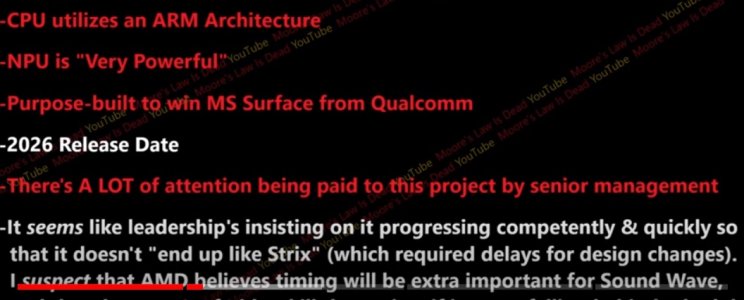
A LOT attention being paid by senior management? Of course, this is first ARM SoC from AMD to compete with next gen mainstream computers. Not low power 2+4 CPU with 4CU GPU, Jesus....
To win Surface from Qualcomm? How? Qualcomm has 5G modem which has started integrated with SoC like X2-EE?
Answer: To license 5G modem IP from Samsung and integrate with Soundwave.
Why timing is extra important for Soundwave?
Answer: Cause AMD, NV, Mediatek, Samsung and Qualcomm are all going on-stage to unveil their ARM solutions togethers under Windows on ARM 12 announcement.
When AMD signed a deal with Samsung supplying Radeon IP to Exynos series, what do AMD gets in return beside new competitor in PC market? Well, AMD will get 5G Modem IP from Samsung. Thanks to the table above, I think AMD will integrate 5G modem inside Soundwave 200mm2 SoC just like X2 series.
Yes, 5G modem integration is next frontier of mobile computing. Qualcomm, Mediatek and Samsung have been doing it for their phone SoC. It is times for mobile computing. That's why NV and AMD are partnering with Mediatek and Samsung to offer total solution for PC market. If you are old enough to remember Centrino with WiMax solution, here comes Centrino 5G moment. We are finally getting real full day battery life with Internet connectivity anywhere. Please checkout HP Go package, I think this is the feature Apple is working with their C1 modem too.
X2-Elite with 128-bit memory bus is way too power hungry for Surface Pro. So, what Soundwave features will standout compared to upcoming Qualcomm X2 SoC? Otherwise, how could Microsoft switch to AMD's Soundwave? 😎
Thanks @marees for the like of old thread below:

A LOT attention being paid by senior management? Of course, this is first ARM SoC from AMD to compete with next gen mainstream computers. Not low power 2+4 CPU with 4CU GPU, Jesus....
To win Surface from Qualcomm? How? Qualcomm has 5G modem which has started integrated with SoC like X2-EE?
Answer: To license 5G modem IP from Samsung and integrate with Soundwave.
Why timing is extra important for Soundwave?
Answer: Cause AMD, NV, Mediatek, Samsung and Qualcomm are all going on-stage to unveil their ARM solutions togethers under Windows on ARM 12 announcement.
When AMD signed a deal with Samsung supplying Radeon IP to Exynos series, what do AMD gets in return beside new competitor in PC market? Well, AMD will get 5G Modem IP from Samsung. Thanks to the table above, I think AMD will integrate 5G modem inside Soundwave 200mm2 SoC just like X2 series.
Yes, 5G modem integration is next frontier of mobile computing. Qualcomm, Mediatek and Samsung have been doing it for their phone SoC. It is times for mobile computing. That's why NV and AMD are partnering with Mediatek and Samsung to offer total solution for PC market. If you are old enough to remember Centrino with WiMax solution, here comes Centrino 5G moment. We are finally getting real full day battery life with Internet connectivity anywhere. Please checkout HP Go package, I think this is the feature Apple is working with their C1 modem too.
X2-Elite with 128-bit memory bus is way too power hungry for Surface Pro. So, what Soundwave features will standout compared to upcoming Qualcomm X2 SoC? Otherwise, how could Microsoft switch to AMD's Soundwave? 😎
Last edited:
XDNA3 For SWV (~80 TOPS) and Medusa Premium (~110 TOPS)
MLID leaked: Soundwave's NPU is very powerful. What does it mean in technical term? Hoho, I think I managed to calculate how powerful is upcoming XDNA3 below:
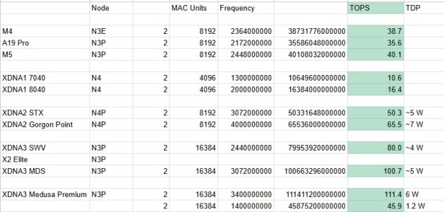
The TOPS are depending on the amount of MAC units x Frequency. It is so simple to calculate; that's why all OEMs are not willing to share the MAC units and clock speeds. Luckily, we got leaks about M4's NPU clock speed @ 2364MHz and AMD XDNA1's clock speed @ 1.3GHz. That's why I could complete my calculation above. STX's XDNA2 TOPS has been tripled due to doubling of MAC units and clockspeed.
The upcoming Soundwave will double the MAC units to 16384, the same as Medusa Premium. Thanks to MLID, we know Medusa Premium's SoC could have up to 110 TOPS: that's mean AMD will clock the MAC units up to 3.4GHz @ 6W. By reducing the frequency down to 1.4GHz, XDNA3 TOPS could have been down to 46TOPS @ 1.2W. Soundwave's NPU should be clocked at least 2.44GHz to meet the requirement of upcoming Windows Co-pilot, which is similar to 2.364GHz of M4's NPU because they are both target at same market.
MLID leaked: Soundwave's NPU is very powerful. What does it mean in technical term? Hoho, I think I managed to calculate how powerful is upcoming XDNA3 below:

The TOPS are depending on the amount of MAC units x Frequency. It is so simple to calculate; that's why all OEMs are not willing to share the MAC units and clock speeds. Luckily, we got leaks about M4's NPU clock speed @ 2364MHz and AMD XDNA1's clock speed @ 1.3GHz. That's why I could complete my calculation above. STX's XDNA2 TOPS has been tripled due to doubling of MAC units and clockspeed.
The upcoming Soundwave will double the MAC units to 16384, the same as Medusa Premium. Thanks to MLID, we know Medusa Premium's SoC could have up to 110 TOPS: that's mean AMD will clock the MAC units up to 3.4GHz @ 6W. By reducing the frequency down to 1.4GHz, XDNA3 TOPS could have been down to 46TOPS @ 1.2W. Soundwave's NPU should be clocked at least 2.44GHz to meet the requirement of upcoming Windows Co-pilot, which is similar to 2.364GHz of M4's NPU because they are both target at same market.
Last edited:
NTMBK
Lifer
Okay we can safely disregard the rest thenMLID leaked:
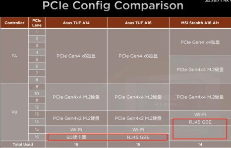
Strix Point 16-lane PCIe 4.0 Configuration
Soundwave Possible PCIe Configuration

Soundwave Possible PCIe Configuration
| Controller | STX PCIe 4.0 | Qualcomm X2-EE | PTH-H 12Xe | Soundwave / M5? | ||
|---|---|---|---|---|---|---|
| PA | 1 PCIe Gen4 | 1 PCIe Gen5 | 1 PCIe Gen5 | |||
| 2 PCIe Gen4 | 2 PCIe Gen5 | 2 PCIe Gen5 | ||||
| 3 PCIe Gen4 | 3 PCIe Gen5 | 3 PCIe Gen5 | PCIe Gen5 x 4 SSD | |||
| 4 PCIe Gen4 | 4 PCIe Gen5 | 4 PCIe Gen5 | ||||
| 5 PCIe Gen4 | 5 PCIe Gen5 | |||||
| 6 PCIe Gen4 | 6 PCIe Gen5 | |||||
| 7 PCIe Gen4 | 7 PCIe Gen5 | |||||
| 8 PCIe Gen4 | 8 PCIe Gen5 | |||||
| PB | 9 PCIe Gen4 | 9 PCIe Gen5 | 5 PCIe Gen4 | |||
| 10 PCIe Gen4 | 10 PCIe Gen5 | 6 PCIe Gen4 | ||||
| 11 PCIe Gen4 | 11 PCIe Gen5 | 7 PCIe Gen4 | PCIe Gen4 x 4 SSD / Thunderbolt 4 | |||
| 12 PCIe Gen4 | 12 PCIe Gen5 | 8 PCIe Gen4 | ||||
| 13 PCIe Gen4 | 13 PCIe Gen4 | 9 PCIe Gen4 | Wi-Fi + BT | |||
| 14 PCIe Gen4 | 14 PCIe Gen4 | 10 PCIe Gen4 | SD Card Reader | |||
| 15 PCIe Gen4 | 15 PCIe Gen4 | 11 PCIe Gen4 | RJ45 GBE | |||
| 16 PCIe Gen4 | 16 PCIe Gen4 | 12 PCIe Gen4 |
Last edited:
Why does Apple still keep Neural Engine in M5?XDNA3 For SWV (~80 TOPS) and Medusa Premium (~110 TOPS)
MLID leaked: Soundwave's NPU is very powerful. What does it mean in technical term? Hoho, I think I managed to calculate how powerful is upcoming XDNA3 below:
View attachment 132486
The TOPS are depending on the amount of MAC units x Frequency. It is so simple to calculate; that's why all OEMs are not willing to share the MAC units and clock speeds. Luckily, we got leaks about M4's NPU clock speed @ 2364MHz and AMD XDNA1's clock speed @ 1.3GHz. That's why I could complete my calculation above. STX's XDNA2 TOPS has been tripled due to doubling of MAC units and clockspeed.
The upcoming Soundwave will double the MAC units to 16384, the same as Medusa Premium. Thanks to MLID, we know Medusa Premium's SoC could have up to 110 TOPS: that's mean AMD will clock the MAC units up to 3.4GHz @ 6W. By reducing the frequency down to 1.4GHz, XDNA3 TOPS could have been down to 46TOPS @ 1.2W. Soundwave's NPU should be clocked at least 2.44GHz to meet the requirement of upcoming Windows Co-pilot, which is similar to 2.364GHz of M4's NPU because they are both target at same market.
With Neural Accelerator (aka NV's Tensor core) feature being introduced in GPU, why don't Apple ditch the Neural Engine aka NPU? According to Bilibili, a lot of AI calculation will benefit from GPU + NA as shown in the graph below:
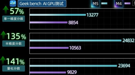
He doesn't really specify the reason for keeping NE. I could guess Apple still has some dedicated features require dedicated NPU. But Apple is not expanding the TOPS of NPU as shown below:
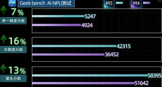
About 7% faster is aligned with my calculation. It seems everybody knows about TOPS formula, but nobody really knows the MAC units and frequency as shown in Hubweb. Hubweb gets the correct clock speed but not the TOPS.
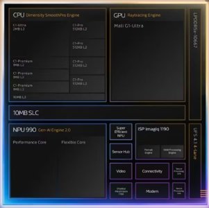
Back to Windows platform, Microsoft is the one who set the rules for Windows. 80TOPS of INT8 NPU should be the standard of Windows 12. Thus all OEMs have to adhere to the standard. As shown in the layout of D9500 below, Mediatek has to spare about 20% of die area (~30mm2) to accommodate 16384 MAC units in order to hit 100TOPS. And if you are studying my table, AMD will introduce XDNA3 with different clock speed and TDP. Soundwave is designed to be power efficient APU, that's why AMD won't set much higher TOPS than 80; unlike Medusa Point and Premium. Hope you guys learned something in TOPS calculation including power TDP. 😎
Oh ya, Nova Lake's NPU6 will most likely comes with 16384 MAC units in order to hit 80TOPS. PTL as usual is one step behind in NPU's TOPS...😛
Last edited:
TRENDING THREADS
-
Discussion Zen 5 Speculation (EPYC Turin and Strix Point/Granite Ridge - Ryzen 9000)
- Started by DisEnchantment
- Replies: 25K
-
Discussion Intel Meteor, Arrow, Lunar & Panther Lakes + WCL Discussion Threads
- Started by Tigerick
- Replies: 25K
-
Discussion Intel current and future Lakes & Rapids thread
- Started by TheF34RChannel
- Replies: 24K
-
-
