Question AMD Phoenix/Zen 4 APU Speculation and Discussion

Page 61 - Seeking answers? Join the AnandTech community: where nearly half-a-million members share solutions and discuss the latest tech.

Exist50

Platinum Member
Aug 18, 2016
2,452
3,106
136
I guess you are talking about a different "different node" than I do. I'm referring to the fact that SRAM scaling has been lackluster for some time and after N5 is essentially dead. So it makes a lot of sense to keep the v-cache die on N5 or older while the main die keeps moving to the latest and greatest (for logic).

Your initial question was:

SRAM mixed with logic is much less dense due to different library used. SRAM using the same latest node as the rest of the logic die ensure increasing amount of expensive area is wasted on SRAM as there is barely any scaling left. Integrating the v-cache capacity into the main die would vastly increase the overall die size, all while the goal is to keep the die size small.

We had that discussion last December already (mainly 1 and 2, more in that Zen 5 thread). You yourself even quoted it back in April.

Bonus: Me answering you in December.
They don't have a different node optimized for SRAM. That's the claim I was referring to. They're just reusing an older node that's cheaper per bit. And you could get the same density on a die that also has logic. Mixing libraries and such is very doable. It's nothing special there.

But on the broader point, I was questioning the value for this approximate gen when they're supposedly still using N4 for the GPU. That still has some SRAM scaling. Of course, long term, the merits of v-cache depend on the cost gap and SRAM density gap between nodes, as well as the overheads of stacking.

But also, v-cache as an additional cache doesn't seem to make sense for a GPU. You'd be better off going all-in if the cost makes sense. Otherwise, you baseline non v-cache SKUs will be memory starved.
 

Bigos

Senior member
Jun 2, 2019
204
519
136
I suspect that a big part of why Apple has designed their L1 cache to be so large is because they want to be able to keep more bits of code from a larger number of applications in the cache so that when people move between them, the performance is much snappier. Their clock speed being more moderate enables this, but there aren't that many applications that need a vast L1 cache whereas every application needs a fast L1 cache. You only really want to increase the size when this can be done without paying any cost to access time. Otherwise it's not worth it.

You are confusing L1 data cache with L1 instruction cache. While both are large on Apple big cores, people usually reference the former when speaking of large L1 cache while the benefits you mention are about the instruction cache.

And L1 instruction cache is too tiny to hold more than one application worth of code, even on Apple cores. This use case of switching between applications would rather make use of large L2+ cache or rather the performance of fetching instructions from L2/L3/memory. Big L1I cache helps individual applications with big executed instruction footprints and modern OOP applications are like that.
 

naukkis

Golden Member
Jun 5, 2002
1,020
853
136
You are confusing L1 data cache with L1 instruction cache. While both are large on Apple big cores, people usually reference the former when speaking of large L1 cache while the benefits you mention are about the instruction cache.

And L1 instruction cache is too tiny to hold more than one application worth of code, even on Apple cores. This use case of switching between applications would rather make use of large L2+ cache or rather the performance of fetching instructions from L2/L3/memory. Big L1I cache helps individual applications with big executed instruction footprints and modern OOP applications are like that.

And holding other applications data doesn't matter at all. Different applications use different virtual memory mappings so data in cache is useless after contex switch until new translations are either made or translation cache is loaded from other caches. And even without that holding other application data in cores private cache would not mean anything in systems which have more than one execution core - that extra cores are there for execute that other application code so back to back switching applications in one core isn't happening. That kind of data sharing happens at system level caches - not in core private caches which nowadays include L2 level too in most designs - not Apple though.
 

moinmoin

Diamond Member
Jun 1, 2017
5,242
8,456
136
They don't have a different node optimized for SRAM. That's the claim I was referring to. They're just reusing an older node that's cheaper per bit. And you could get the same density on a die that also has logic. Mixing libraries and such is very doable. It's nothing special there.

But on the broader point, I was questioning the value for this approximate gen when they're supposedly still using N4 for the GPU. That still has some SRAM scaling. Of course, long term, the merits of v-cache depend on the cost gap and SRAM density gap between nodes, as well as the overheads of stacking.

But also, v-cache as an additional cache doesn't seem to make sense for a GPU. You'd be better off going all-in if the cost makes sense. Otherwise, you baseline non v-cache SKUs will be memory starved.
I honestly don't really follow what's your argument is there. Are you being earnest, or just nitpicking?

You seem to want to err on all-inclusivity, where AMD's approach is to err on creating and retaining as much flexibility as possible. That includes investing in tech like CoW and using it for v-cache even if both combined in a monolithic die could have result in a similar product (but wouldn't have, as AMD strove to keep die sizes down first). Your train of thoughts displayed would have led to AMD staying monolithic for much longer, and a lot of their recent success would likely never happened.

I can image a lot of people at Intel having approached all these topics the way you are here, which would explain very well the mess Intel is still going through currently, neglecting flexible interconnects and packaging techs in favour of more monolithic approaches.
 
  • Like
Reactions: Tlh97 and Joe NYC

Doug S

Diamond Member
Feb 8, 2020
3,574
6,311
136
Next
Big L1I cache helps individual applications with big executed instruction footprints and modern OOP applications are like that.


Nobody has big L1 these days, clock rates are too high and bigger caches introduce too much latency.

Back in the day some L1s were truly massive. HP's PA-8200 had a wave pipelined off chip 2MB L1i & 2MB L1d with 1 cycle latency. Of course it clocked at only 300 MHz, but it kicked serious a** in Oracle type workloads thanks to that huge L1i.
 

Exist50

Platinum Member
Aug 18, 2016
2,452
3,106
136
I honestly don't really follow what's your argument is there. Are you being earnest, or just nitpicking?

You seem to want to err on all-inclusivity, where AMD's approach is to err on creating and retaining as much flexibility as possible. That includes investing in tech like CoW and using it for v-cache even if both combined in a monolithic die could have result in a similar product (but wouldn't have, as AMD strove to keep die sizes down first). Your train of thoughts displayed would have led to AMD staying monolithic for much longer, and a lot of their recent success would likely never happened.

I can image a lot of people at Intel having approached all these topics the way you are here, which would explain very well the mess Intel is still going through currently, neglecting flexible interconnects and packaging techs in favour of more monolithic approaches.
My point is that flexibility, i.e. having optional v-cache, only has value if you actually use that flexibility, and for a GPU within the next year or so, it seems that a Ryzen-like v-cache solution would not yield two independently viable and distinct products. By contrast, AMD's CPU chiplets are great, because they can reuse them across the lineup, and reuse the IO die across gens with different CPU dies.

And monolithic vs chiplet is not why Intel's having trouble. Meteor Lake has everything you seem to want, and that program has been a dumpster fire. Having clean, modular interfaces is part of the problem, but that applies to chiplet or monolithic.
 
  • Like
Reactions: Tlh97 and Geddagod

Geddagod

Golden Member
Dec 28, 2021
1,524
1,620
106
Well even if true, that doesn't harm my point...

But I guess we'll see what they come out with.
I heard that the MCDs have TSV's as well.
But ye I agree, if the stacked cache would have improved the performance and efficiency of RDNA3 to the point they could make it into a viable flagship, then I don't really doubt AMD wouldn't have done it, just for the halo 'mindshare' sku
 

adroc_thurston

Diamond Member
Jul 2, 2023
7,094
9,850
106
Well even if true, that doesn't harm my point...
Stacked MCDs weren't a product since N31 itself is way below target due to gfx clock miss.
if the stacked cache would have improved the performance and efficiency of RDNA3 to the point they could make it into a viable flagship
Was mostly about high-res leadership, they had a real™ flagship in a different part which got canned anyway.
 

moinmoin

Diamond Member
Jun 1, 2017
5,242
8,456
136
Having clean, modular interfaces is part of the problem, but that applies to chiplet or monolithic.
It's only the very starting point to modularizing the design if not a prerequisite. That Intel somehow thought that can be skipped or glossed over is worrying enough.

I'm looking forward to the MTL "dumpster fire" scaling up and down Intel's whole product range. That's the kind of flexibility I'm looking for, not modularization for the sake of it (that we saw with Lakefield already). ;)

We had people raving about Infinity Fabric for ages. Intel had Keller on its payroll for some time. Is that whole topic really still an unresolved one over there after 6 years?
 

MadRat

Lifer
Oct 14, 1999
11,999
307
126
Some crazy talk goes on when people talk about AMD and the size of their L1. Large L1 caches are a luxury, not a compromise. Having a bump in L1 will mean a successful higher hit rate of a very important small percent increase for minimal penalty in latency gain. Every other level of cache will have much higher penalty. Intel has a substantially larger L1 and its been one of their big advantages over AMD.
 

JoeRambo

Golden Member
Jun 13, 2013
1,814
2,105
136
Some crazy talk goes on when people talk about AMD and the size of their L1. Large L1 caches are a luxury, not a compromise. Having a bump in L1 will mean a successful higher hit rate of a very important small percent increase for minimal penalty in latency gain.

"Minimal penalty" ? Are we serious now, Intel has 5 cycle 48KB D L1, AMD has 4 cycle 32KB D L1. It is tradeoff of 50% more size for 25% more latency, not minimal at all.
 

Joe NYC

Diamond Member
Jun 26, 2021
3,647
5,186
136
My point is that flexibility, i.e. having optional v-cache, only has value if you actually use that flexibility, and for a GPU within the next year or so, it seems that a Ryzen-like v-cache solution would not yield two independently viable and distinct products. By contrast, AMD's CPU chiplets are great, because they can reuse them across the lineup, and reuse the IO die across gens with different CPU dies.

And monolithic vs chiplet is not why Intel's having trouble. Meteor Lake has everything you seem to want, and that program has been a dumpster fire. Having clean, modular interfaces is part of the problem, but that applies to chiplet or monolithic.
AMD APUs are by far the worst example of modularity - basically none as far as re-using dies. This is costly and it sucks / wastes resources.

The other end of the spectrum, modularity and re-usability - modularity nirvana - would have CPU CCD dies that are shared with desktop and server and GPU GCD dies that are shared with dGPUs.

IMO, the ultimate goal for AMD is to reach this nirvana.

We will see if either Strix Halo or RDNA 4 offer us any clues of how AMD is planning on getting there...
 

adroc_thurston

Diamond Member
Jul 2, 2023
7,094
9,850
106
AMD APUs are by far the worst example of modularity - basically none as far as re-using dies
Die reuse is a meme at mobile volumes.
IP reuse, though, is king.
would have CPU CCD dies that are shared with desktop and server and GPU GCD dies that are shared with dGPUs.
Those are all entirely different markets with little overlaps with mobile.
Stop.
We will see if either Strix Halo or RDNA 4 offer us any clues of how AMD is planning on getting there...
I can safely say they do not.
 

Exist50

Platinum Member
Aug 18, 2016
2,452
3,106
136
AMD APUs are by far the worst example of modularity - basically none as far as re-using dies. This is costly and it sucks / wastes resources.

The other end of the spectrum, modularity and re-usability - modularity nirvana - would have CPU CCD dies that are shared with desktop and server and GPU GCD dies that are shared with dGPUs.

IMO, the ultimate goal for AMD is to reach this nirvana.

We will see if either Strix Halo or RDNA 4 offer us any clues of how AMD is planning on getting there...
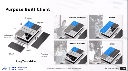
I think the ultimate goal would be similar to this graphic that (somewhat ironically) Intel showed some years back. Not just CCD level granularity, but core level granularity.

1689055549427.png

Of course, practically speaking, there are a whole host of challenges to such an idea, and it's for many of the same reasons that you don't see 100% reuse of dies even today. There're always going to be tradeoffs that make sense for one market but not another.

Like, you call the monolithic APU dies a waste, but clearly Dragon Range shows there are challenges with just reusing their existing compute dies. Mobile is certainly high enough volume to justify the extra design/manufacturing effort. Maybe future packaging breakthroughs can help close the gap.
 

moinmoin

Diamond Member
Jun 1, 2017
5,242
8,456
136
In my opinion the main thing about modularization is the tradeoff between die size and overhead, i.e. area needed for additional I/O necessary to connect the broken up dies. AMD stated that with Zeppelin the overhead was ~10% that could have been saved going monolith. With SPR with its abundant use of EMIB the overhead is around ~21%.

So the smaller the pieces, the more pieces, and/or the faster the interconnect the bigger the overhead likely is to be.

APUs for mobile are ideally small in area for mass production, power efficiency and cost. Whether there truly ever is a chiplet strategy that works well within those limits remains to be seen. Personally I expect monolithic dies to remain relevant at the lowest end. The product range split between Phoenix and Dragon Range already shows where that line may be drawn even in the future.
 

adroc_thurston

Diamond Member
Jul 2, 2023
7,094
9,850
106
In my opinion the main thing about modularization is the tradeoff between die size and overhead, i.e. area needed for additional I/O necessary to connect the broken up dies
Ehhhh that's mostly for 2.5D/2D stuff.
3D tiling costs very little for the compute part since you can directly hook your favourite CMOS buses in.
Whether there truly ever is a chiplet strategy that works well within those limits remains to be seen.
Well I mean STX-Halo is a 2.5D big boy APU from AMD so it really does, just not everywhere.
 
  • Like
Reactions: Tlh97 and Joe NYC

TESKATLIPOKA

Platinum Member
May 1, 2020
2,696
3,260
136
MLD claimed 2.5 months ago that STX-Halo has 16 Zen5 cores + 40CU IGP(GPU) + 32MB cache + 256bit LPDDR5x, don't know what is true and what is not.
If It really has LPDDR5(x) then we can forget about expanding memory and there is still the question about price of this product.
 

Doug S

Diamond Member
Feb 8, 2020
3,574
6,311
136
In my opinion the main thing about modularization is the tradeoff between die size and overhead, i.e. area needed for additional I/O necessary to connect the broken up dies. AMD stated that with Zeppelin the overhead was ~10% that could have been saved going monolith. With SPR with its abundant use of EMIB the overhead is around ~21%.

So the smaller the pieces, the more pieces, and/or the faster the interconnect the bigger the overhead likely is to be.

APUs for mobile are ideally small in area for mass production, power efficiency and cost. Whether there truly ever is a chiplet strategy that works well within those limits remains to be seen. Personally I expect monolithic dies to remain relevant at the lowest end. The product range split between Phoenix and Dragon Range already shows where that line may be drawn even in the future.


Two monolithic dies (one smaller one bigger) would serve 90% of PC buyers. The modular solutions really only make sense for those in the niches, and even then I'm skeptical whether a corporate power user is all that different from a gamer or creator. And who the hell knows what a "mobile go-getter" is lol

They try to show some sort of usefulness for this modularity in tailoring specific solutions, but whoever did it obviously doesn't understand their markets at all. Why would corporate users want on chip AI? Whereas individuals with privacy concerns want AI to be done locally rather than in the cloud, that objection doesn't exist for corporate users. Their IT department would have them do all their AI tasks in the corporate cloud, and save money buying PCs for every employee without any on chip AI that would sit idle 99.99% of the time. They will want those AI tiles on their server CPUs, not client CPUs.

And why do they show a gamer with all GPU/CPU and no AI or I/O? They don't need AI cores today because they don't have them so games aren't written to use them. I wonder, do iOS games use the NPU at all? I'd be surprised if there weren't a few big name games that do...because they can count on it being there in every single iPhone sold in the past half decade or so. If gamers start buying CPUs with AI cores someone will write a game that exploits that resource.
 

Joe NYC

Diamond Member
Jun 26, 2021
3,647
5,186
136
Die reuse is a meme at mobile volumes.
IP reuse, though, is king.

AMD does not really have the volumes at which creating new dies with all their associated costs is a rounding error.

Also, the thread of messages touched above on APUs that could encroach on the territory of notebooks with a separate dGPU die.