Question AMD Phoenix/Zen 4 APU Speculation and Discussion

Page 60 - Seeking answers? Join the AnandTech community: where nearly half-a-million members share solutions and discuss the latest tech.

Mopetar

Diamond Member
Jan 31, 2011
8,487
7,726
136
I think there's a big market for a halo APU. All of those x50 and x60 series GPUs in a laptop could be replaced with a sufficiently big APU, and the integrated cost and power advantage would really help compete with Nvidia.

I do think there is a market here. It's just a matter of what it costs as the market doesn't want to pay for a $500 APU.

I don't think vcache makes as much sense for APUs right now. Would it provide an advantage vs applying the same incremental cost to other components? Also, laptops run hotter, so that lower thermal limit might be a problem.

I think that it does make a certain amount of sense as v-cache doesn't like higher voltage which limits the power usage so it's less of a big deal for notebooks.

The other reason I think it's advantageous is that an APU is sharing system and video memory over the same bus and it's significantly less than what a dedicated GPU will have. If the CPU could share that extra cache with the graphics cores so it was basically an infinity cache when needed it would likely add more performance than just about anything else. It doesn't make the base die all that much larger either.
 
  • Like
Reactions: Joe NYC

Exist50

Platinum Member
Aug 18, 2016
2,452
3,106
136
It's just a matter of what it costs as the market doesn't want to pay for a $500 APU.
Well, that depends. If that $500 APU provides the same performance as a $300 CPU + $400 GPU (just for illustration's sake), then that's still a great value proposition. But whatever the exact numbers may be, I think the sweet spot will be that --60 tier mainstream gaming/productivity thin and light. I think the higher end of the market would be too difficult to challenge for an iGPU.
If the CPU could share that extra cache with the graphics cores so it was basically an infinity cache when needed it would likely add more performance than just about anything else.
So then the question I propose is why not just integrate that v-cache capacity into the main die? Is there a scenario where you'd want a SKU without it? I don't think the packaging costs are yet low enough to be cheaper than monolithic, or are they?
It doesn't make the base die all that much larger either.
So is your thought to have the cache as a base die? Or was this more in the context of something like Meteor/Arrow Lake topology?
 
  • Like
Reactions: Joe NYC

uzzi38

Platinum Member
Oct 16, 2019
2,746
6,653
146
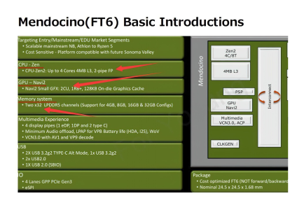
It's presumably supposed to compete with Intel's 2+8 U series chips around 15W. ADL 2+8 is in a ton of devices, and it makes sense for AMD to put out more dies to better match the price point and power envelope.

Mendocino is more of a cost-focused product, and doesn't have a clear successor yet. I think eventually we'll see something with 4x Zen 4c on N4, but that's just a guess.
The follow up for Mendocino is Sonoma Valley, it's already been rumoured thanks to a leaked diagram at some point back around the time rumours for Mendocino started popping up.

As for what it is though, not much is publicly known for now.
 
  • Like
Reactions: Tlh97 and Exist50

Kepler_L2

Senior member
Sep 6, 2020
998
4,262
136
There's also PHX2e/BDT, though that seems to be more of a Van Gogh successor than a Mendocino one.
 

SpudLobby

Golden Member
May 18, 2022
1,041
702
106
I think it's interesting to speculate where they'd draw the cutlines for such a product. I know there are rumors claiming a big GPU+AI+IO die, with reused compute dies, and I guess that sounds fine for a really high end product, but I agree it would be interesting to see something from the other direction with a mobile-derived CPU+IO complex and another die for GPU and maybe AI. Or something like Intel's SoC cores might be interesting, but that'll probably come after they have hybrid better established.
Yeah, pretty much. I suppose approaching from the other end and down may well still provide value for gamers on the desktop or in 80W+ gaming laptops, there's no doubt the APU approach is probably going to be more and more common in the future IMO. There are ways to win either way.

But for mobile specifically I suppose I am not especially interested in some monstrosity from AMD that doesn't have an integrated CPU die and/or suffers from piss poor idle power because it's ultimately about replacing dGPU's + Dragon Range type stuff. That's cool and all, great even, but meh. Arrow Lake with a wider bus or a Strix Point derivative with a wider bus and then I'm curious.
 

deasd

Senior member
Dec 31, 2013
603
1,033
136
Some PHX2 rumors from TPU Mod


Phoenix-2 doesn't have any "Zen 4c" cores. There's just one CCX with 6x "Zen 4" cores. The L3$ size is reduced to 8 MB, but there's no confirmation of this.
 

uzzi38

Platinum Member
Oct 16, 2019
2,746
6,653
146
@deasd I'm gonna be honest, AFAIK that guy is the one that makes all the rumour mill articles, I don't think he actually knows more than what the rumour mill says.

Not saying it is or it isn't: I'd like to make it clear I don't know how the L3 is arranged. But I also am not sure I would assume what they've said is correct.
 

Mopetar

Diamond Member
Jan 31, 2011
8,487
7,726
136
So then the question I propose is why not just integrate that v-cache capacity into the main die?

To keep the size of the main die smaller. An APU is already quite a bit larger than any of the individual components would be using a chiplet approach and 64 MB of SRAM isn't exactly negligible in terms of die area. The v-cache chiplet can at least use a different node so it can be denser. Any added cost of bonding is going to be less than the larger dies you'd need otherwise. If they can reuse the same cache chiplets it doesn't add much to production costs or risk overproduction.

Is there a scenario where you'd want a SKU without it? I don't think the packaging costs are yet low enough to be cheaper than monolithic, or are they?

Market segmentation mainly, but APUs being larger dies means a lower yield and having mor dimensions to bin on. You would only want the top performing chips to get v-cache. Not much sense in adding it to the ones that are going to have disabled GPU cores.
 
  • Like
Reactions: moinmoin

Exist50

Platinum Member
Aug 18, 2016
2,452
3,106
136
Any added cost of bonding is going to be less than the larger dies you'd need otherwise.
That, I think, is an assumption we'll need to see tested. It's not like they have a separate node tailored just for SRAM, so it's mainly a question of yield tradeoffs with a bigger die vs packaging loss.
Market segmentation mainly, but APUs being larger dies means a lower yield and having mor dimensions to bin on. You would only want the top performing chips to get v-cache. Not much sense in adding it to the ones that are going to have disabled GPU cores.
They don't really need to cut down consumer-class GPUs much. Tend to be on relatively mature process.
 

Mopetar

Diamond Member
Jan 31, 2011
8,487
7,726
136
That, I think, is an assumption we'll need to see tested. It's not like they have a separate node tailored just for SRAM, so it's mainly a question of yield tradeoffs with a bigger die vs packaging loss.

They're already doing this to some extent with the v-cache which is made using a different set of design libraries to achieve better density since the cache chiplet is just cache. On the GPU side the infinity cache and memory controller that sit on the MCM chiplet are made on the older 6nm process node since there's not much scaling benefit for going down to 5nm for that chiplet.

TSMC has said that some of their different nodes are designed to work with each other so that not every layer of stacked silicon needs to be in the same node. I would imagine that AMD has been experimenting with this since the cost savings could be rather significant given the cost of wafers on the bleeding edge.
 

moinmoin

Diamond Member
Jun 1, 2017
5,242
8,456
136
It's not like they have a separate node tailored just for SRAM
Considering that SRAM scaling is already stagnating they actually already do, yes. And that's not even considering the library optimized for SRAM use that allows much denser SRAM dies than SRAM intermixed with logic even on the same node.
 

MadRat

Lifer
Oct 14, 1999
11,999
307
126
I will be disappointed if they don't expand L1 caches. The single most effective cache is L1. Seems pointless to overload a long in the tooth L1 design with each Zen# release.
 

Geddagod

Golden Member
Dec 28, 2021
1,524
1,620
106
80 KB L1 was what was leaked right? What's that config going to be, 48+32?
I'm curious about what's going to be the bigger cache, L1D or L1I.
 

adroc_thurston

Diamond Member
Jul 2, 2023
7,094
9,850
106
Thought the biggest impact was the latency hit not the clock speed
Apple does gigantic L1 caches with 3 cycle load to use latency so yes, it's literally all about clock speeds, latency included.

Again, the improvements in Zen5 are genuinely too numerous to count, focusing on L1$ alone is silly.
 
  • Like
Reactions: Tlh97

Geddagod

Golden Member
Dec 28, 2021
1,524
1,620
106
Apple does gigantic L1 caches with 3 cycle load to use latency so yes, it's literally all about clock speeds, latency included.
Huh forgot about that. But didn't WLC just trade off 1? extra cycle of latency for maintaining ~same peak clocks as SKL? Seems like you could trade off either, though I might be mistaken in my assumption that the latency hit is more impactful than the frequency hit.
 

adroc_thurston

Diamond Member
Jul 2, 2023
7,094
9,850
106
But didn't WLC just trade off 1? extra cycle of latency for maintaining ~same peak clocks as SKL?
That they did.
though I might be mistaken in my assumption that the latency hit is more impactful than the frequency hit.
It's all a chain of very careful tradeoffs.
Lightning (A13 big core) was the last one to bump L1i in Apple lands and in that was a PPW regression over Vortex (A12 big core) all for some measely 13% IPC bump.
 
  • Like
Reactions: Tlh97 and moinmoin

Exist50

Platinum Member
Aug 18, 2016
2,452
3,106
136
TSMC has said that some of their different nodes are designed to work with each other so that not every layer of stacked silicon needs to be in the same node.
I assume that to refer to the fact that you need to put some consideration into the top metal layer to support hybrid bonding. IIRC, TSMC only supports a small number of combinations at this time.
Considering that SRAM scaling is already stagnating they actually already do, yes.
Do you have any source for the node itself being different? Design optimization and library choice, sure, but I haven't seen any indication that TSMC customized the node for SRAM.
 

moinmoin

Diamond Member
Jun 1, 2017
5,242
8,456
136
Do you have any source for the node itself being different? Design optimization and library choice, sure, but I haven't seen any indication that TSMC customized the node for SRAM.
I guess you are talking about a different "different node" than I do. I'm referring to the fact that SRAM scaling has been lackluster for some time and after N5 is essentially dead. So it makes a lot of sense to keep the v-cache die on N5 or older while the main die keeps moving to the latest and greatest (for logic).

Your initial question was:
So then the question I propose is why not just integrate that v-cache capacity into the main die?
SRAM mixed with logic is much less dense due to different library used. SRAM using the same latest node as the rest of the logic die ensure increasing amount of expensive area is wasted on SRAM as there is barely any scaling left. Integrating the v-cache capacity into the main die would vastly increase the overall die size, all while the goal is to keep the die size small.

We had that discussion last December already (mainly 1 and 2, more in that Zen 5 thread). You yourself even quoted it back in April.

Bonus: Me answering you in December.
GAA should improve it again, to be seen by how much. But until then calling it dead is apt. SRAM not scaling makes it very expensive to keep at the same size, nevermind increase in size. No more doubling of cache sizes on monolithic dies. Moving SRAM to a separate die on N5 or older is the only economical solution.
 
Last edited:

Mopetar

Diamond Member
Jan 31, 2011
8,487
7,726
136
Depending on how the cache is laid out, you can increase the capacity without impacting the clock speeds overly much, but there are design trade offs.

Probably the easiest change would be to double the line length, which wouldn't affect the timing too much assuming you double the bus size so that loading or evicting an entry doesn't take any longer. Of course that bigger bus is more power hungry and needs more transistors.

Of course there's probably not that much of a performance uplift from increasing the line size. Most x86 CPUs have been using 64 byte cache lines for decades. If there was a big enough performance gain to justify doubling it, someone would have done so by now.

I suspect that a big part of why Apple has designed their L1 cache to be so large is because they want to be able to keep more bits of code from a larger number of applications in the cache so that when people move between them, the performance is much snappier. Their clock speed being more moderate enables this, but there aren't that many applications that need a vast L1 cache whereas every application needs a fast L1 cache. You only really want to increase the size when this can be done without paying any cost to access time. Otherwise it's not worth it.