
64 core EPYC Rome (Zen2)Architecture Overview?
Page 28 - Seeking answers? Join the AnandTech community: where nearly half-a-million members share solutions and discuss the latest tech.
You are using an out of date browser. It may not display this or other websites correctly.
You should upgrade or use an alternative browser.
You should upgrade or use an alternative browser.
Enjoy...
2.5GHz, curiously that s about 13.6% over an Epyc 7601, as much as the alleged IPC improvement stated by BitsChips.
Zapetu
Member
- Nov 6, 2018
- 94
- 165
- 66
Enjoy...
2.35GHz 64c unknown rome vs highest freq 32 core 7601 that tops out at at 2.2GHz.
We need to know tdp but they hardly cant push 4 times as much fp at same tdp.
Shouldn't TDP be the same 180W assuming socket and MB compability? Or am I missing something here and super computers have different TDP requirements.
https://www.datacenterdynamics.com/news/24-petaflop-hpe-supercomputer-feature-amd-epyc-rome-cpus/
640.000 cores means 10.000 processors and since there are 5000 nodes, this is build with 2S systems. There might be no need for AMD to even consider 4S and beyond, or would there be any benefits to that? They seem to do just fine with 1S and 2S.
I'm hoping that 2.35Ghz is the base frequency since EPYC 7601 can do 2.7-3.2Ghz turbo:
https://www.anandtech.com/show/13594/amd-launches-highfrequency-epyc-7371-processor
Edit:
https://www.anandtech.com/show/13598/amd-64-core-rome-deployment-hlrs-hawk-at-235-ghz
Last edited:
We need to know tdp but they hardly cant push 4 times as much fp at same tdp.
Considering that supply voltage must go down because of 7nm, there is simply not much room in SP3 to push TDP up.
https://www.anandtech.com/show/13598/amd-64-core-rome-deployment-hlrs-hawk-at-235-ghz
At 2.4 TF/CPU that amount to 37.6GFlops/core or about 15 flops/cycle/core, and that s not even double precision, this is perfectly achievable with FMA and AVX2 full width exe units, i guess that the peak is actually 16 flops/cycle/core.
That gives 2.4 TeraFLOPS per CPU, which likely means there are additional compute accelerators in the system.
At 2.4 TF/CPU that amount to 37.6GFlops/core or about 15 flops/cycle/core, and that s not even double precision, this is perfectly achievable with FMA and AVX2 full width exe units, i guess that the peak is actually 16 flops/cycle/core.
Saylick
Diamond Member
- Sep 10, 2012
- 4,098
- 9,577
- 136
Yeah, 16 SP FLOPS / core / cycle sounds about right: 2.35 GHz x 2 MUL FP units x (256-bit AVX2 / 32-bit SP) x 64 cores = 2.406 TFLOPShttps://www.anandtech.com/show/13598/amd-64-core-rome-deployment-hlrs-hawk-at-235-ghz
At 2.4 TF/CPU that amount to 37.6GFlops/core or about 15 flops/cycle/core, and that s not even double precision, this is perfectly achievable with FMA and AVX2 full width exe units, i guess that the peak is actually 16 flops/cycle/core.
Yeah, 16 SP FLOPS / core / cycle sounds about right: 2.35 GHz x 2 MUL FP units x (256-bit AVX2 / 32-bit SP) x 64 cores = 2.406 TFLOPS
They are almost certainly actually counting 64-bit, but with each FMA as 2 ops. Not that it changes the result.
Vattila
Senior member
- Oct 22, 2004
- 821
- 1,458
- 136
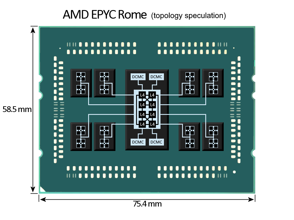
It still may very well be that 14LPP is good enough for their needs and there is no need for a large L4 cache.
If so, it is curious that they wouldn't use 12LP, isn't it? With 12LP libraries they should get 15% better density and better performance (source). In addition, that they state "14nm" (not 14LPP) is a strong hint that they may be using the 14HP process that GlobalFoundries acquired from IBM.
Also Vattila, if you could draw this topology, it would be much appreciated.
Here are some alternative topologies for interconnecting the L4 slices:
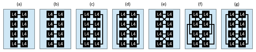
Figures (a-d) are simple textbook topologies; (a) ring, (b) mesh, (c) cube and (d) your twisted cube. Figure (e-g) are variants of mesh and cube topologies, enhanced with direct connections between the nodes in the upper and lower quads: (e) mesh with two fully connected quads, (f) cube with upper and lower sides fully connected, and (g) same cube topology as (f), but with the lower quad flipped vertically.
Topology (f) is used in Naples to connect the chiplets in package and across sockets (illustration). Since it looks like the Rome design is two Naples chips crammed into one socket and optimised, I suspect a similar topology is used for the L4 cache in Rome. Considering the upper and lower halves of the IO chiplet are mirrored in large parts, alternative (g) seems to fit the bill.
Last edited:
PotatoWithEarsOnSide
Senior member
- Feb 23, 2017
- 664
- 701
- 106
H T C
Senior member
- Nov 7, 2018
- 610
- 451
- 136
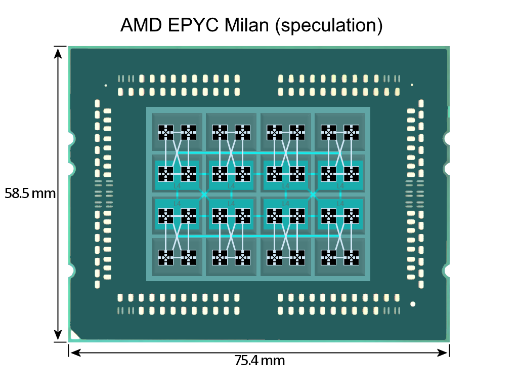
What's the point of introducing IO chiplet in Rome, only to take it away in Milan?
I think Milan will still have the IO chiplet, much like Rome but it should be on an interposer, like in your proposed drawing.
Perhaps instead of 16 dual CCX chiplets, Milan will have 12 dual CCX chiplets. Think your Rome design and add 2 dual CCX chiplets on each side, between the existing CCX chiplets: instead of having 4 dual CCX chiplets on each side of the IO chiplet, it would have 6 dual CCX chiplets.
Thoughts?
Vattila
Senior member
- Oct 22, 2004
- 821
- 1,458
- 136
What's the point of introducing IO chiplet in Rome, only to take it away in Milan?
One way to look at it is that the interposer is the IO chiplet. That said, active interposer and 128 cores in the socket — that is probably pie in the sky for Milan. And when they start designing on active interposers, they may radically change the architecture and topology (ref. research papers by Gabriel Loh). My Milan diagram is just musings on how the current architecture can be extended based on my "quad-tree" ideas — in particular, filling out the current dual-CCX clusters to quads.
Last edited:
Vattila
Senior member
- Oct 22, 2004
- 821
- 1,458
- 136
How, if at all, do these various topologies potentially affect power draw?
This is far beyond my expertise, but I expect a more complex topology to have more overhead due to more complex and more numerous routers. Other than that, it comes down to the type of link and its physical and electrical characteristics (serial/parallel, length, width, impedance, voltage, frequency). Ideally, the network should consume no power if there is no traffic, so power management probably plays a huge part.
First and foremost, I would think that the selection of topology depends on the requirements for bandwidth and latency. Transistor budget for routers and metal layer availability for routing may play a role as well.
Last edited:
Good spotted. You are right ofc - damn i should have seen it even with my limited knowledgeConsidering that supply voltage must go down because of 7nm, there is simply not much room in SP3 to push TDP up.
- makes sense in the grander scene anyway to keep same tdp. Well if 2.35 is base then certainly we are in for some crazy fp numbers then.
Last edited:
Zapetu
Member
- Nov 6, 2018
- 94
- 165
- 66
It still may very well be that 14LPP is good enough for their needs and there is no need for a large L4 cache.
If so, it is curious that they wouldn't use 12LP, isn't it? With 12LP libraries they should get 15% better density and better performance (source). In addition, that they state "14nm" (not 14LPP) is a strong hint that they may be using the 14HP process that GlobalFoundries acquired from IBM.
They didn't utilize that 15% better density in Pinnacle Ridge at all and, as far as we know, the upcoming Polaris 30 don't do that either. So they only ever used that node for a little better performance.
But I agree that 14HP would be a much better option (because of eDRAM) for their chiplets + IO die design than 14LPP. Only pros for 14LPP would be guaranteed capacity and availability (and lower cost). If IBM allows it, 14HP is the best possible option AMD has for the IO die. Since chiplet-to-IO die IF-link will have a significant latency penalty (there are no miracles here with the organic packaging), they need all the buffers and L4 cache that 14HP would alllow.
There are two opinions on this subject where some say that all the IO will take too much space to be able to fit any kind of large L4 and others, myself included, find it hard to believe that this design would offer any performance gains without some secret sauce which would be 14HP and all the possibilities it brings.
I was just wondering about 14LPP since Beemster was considering the possibility that IBM may not allow AMD to use "their" 14HP lithography process (here and later here). I also don't see how this design would be any good with just using 14LPP, but then again, I could also be wrong since I'm not seeing the whole picture. One possibility could be that IBM and AMD are helping each other where AMD gets to use 14HP and maybe IBM needs some assistance with Power10 which might have some kind of chiplet design also. That's pure speculation based on no facts, though, since Power9 is a monolithic design which relies heavily on custom 14HP process. But since GloFo won't develop any smaller lithography processes in the foreseeable future, IBM has to adapt and in the sense go fabless as AMD has done. They (IBM) can still use 14HP for some parts of their design as AMD hopefully will also be able to do.
So to be clear, I'm still strongly in the 14HP camp until otherwise proven.
Edit: I know that IBM has been fabless since 2015 but not too long ago they were still relying on GloFo to develop their own custom smaller lithography processes. And since they like eDRAM so much, it might not be so easy to adapt. I don't see 7 nm processes supporting eDRAM and neither 10 nm processes.
Last edited:
Vattila
Senior member
- Oct 22, 2004
- 821
- 1,458
- 136
Perhaps instead of 16 dual CCX chiplets, Milan will have 12 dual CCX chiplets. Think your Rome design and add 2 dual CCX chiplets on each side
Yeah, I see. You may be able to extend the Rome design by cramming in another two 8-core chiplets on each side of the IO chiplet, provided the package substrate has the metal layers and space for the IF links. The L4 cache would grow by 50%, both in size and the number of slices. With more nodes in the L4 you probably need a change in topology, and you might get worse latency. The size of the L4 would probably no longer fit in a 14nm IO chiplet of the same size, and a bigger chiplet may not fit in the package. One crazy solution may be to move the L4 cache to a 7nm chiplet mounted on top of the 14nm IO chiplet. Then the footprint of the IO chiplet could come down dramatically.
Zapetu
Member
- Nov 6, 2018
- 94
- 165
- 66
Here are some alternative topologies for interconnecting the L4 slices:
Very nice. Choosing the right topology isn't everything, though, and the implementation matters even more. All topologies have their limitations but Intel's ring bus can sure support more cores (up to a point) in a more uniform way than AMD's CCXs connected through Infinity Fabric. To be honest, it has more to do with monolithic vs. MCM design than with anything else, although topologies do matter. I'm sure that there are many improvements AMD has made in IF 2.0 since there are at least a few weak points in their first take on it.
To be exact, Mark didn't say that they would get rid of NUMA like behavior altogether, he just said that the latencies would be more uniform and more predictable. There must be some big latency improvements in chiplet-to-IO die IF-links and memory controllers for general improvement in memory latencies over Naples.
IC: With all the memory controllers on the IO die we now have a unified memory design such that the latency from all cores to memory is more consistent?
MP: That’s a nice design – I commented on improved latency and bandwidth. Our chiplet architecture is a key enablement of those improvements.
IC: When you say improved latency, do you mean average latency or peak/best-case latency?
MP: We haven’t provided the specifications yet, but the architecture is aimed at providing a generational improvement in overall latency to memory. The architecture with the central IO chip provides a more uniform latency and it is more predictable.
(f) cube with upper and lower sides fully connected, and (g) same cube topology as (f), but with the lower quad flipped vertically.
The difference between topologies (f) and (g) comes into the picture when you look at them on a 2D plane. Then (f) should have shorter (and more uniform) physical distances between longer hops and should therefore likely be preferred on-die. For illustrations they are practically the same if you assume that all L4 slices are equal.
Topology (f) is used in Naples to connect the chiplets in package and across sockets (illustration). Since it looks like the Rome design is two Naples chips crammed into one socket and optimised, I suspect a similar topology is used for the L4 cache in Rome. Considering the upper and lower halves of the IO chiplet are mirrored in large parts, alternative (g) seems to fit the bill.
Right. It's one fairly balanced possibility. Some kind of eDRAM buffer could also be attached directly to memory controllers/in each MC, we don't know for sure. Hope AMD still has the ability to use 14HP process to do such things without using too much space.
Also the updated EPYC Rome (topology speculation) looks much more balanced because the topology inside IO die now has diameter of 2 instead of 3. It's still not at all clear how they circumvented all those possible latency issues related to their chiplets + IO die design.
Last edited:
Gideon
Platinum Member
- Nov 27, 2007
- 2,039
- 5,071
- 136
Hmm, A High-Speed Napels based CPU arriving in 2019Q1 and Some EPYC PCIe v4 motherboards arriving in Q3. Points pretty clearly towards a possible launch somewhere in Q2 with mass-availability in Q3.
Hmm, A High-Speed Napels based CPU arriving in 2019Q1 and Some EPYC PCIe v4 motherboards arriving in Q3. Points pretty clearly towards a possible launch somewhere in Q2 with mass-availability in Q3.
Could just be that the Cloud Companies are going to get the first wave exclusively and you won't see any OEM products until Q3.
DrMrLordX
Lifer
- Apr 27, 2000
- 23,088
- 13,185
- 136
Could just be that the Cloud Companies are going to get the first wave exclusively and you won't see any OEM products until Q3.
Intel has done that before. I'm pretty sure Google and Amazon got first crack at Skylake-SP.
Beemster
Member
- May 7, 2018
- 34
- 30
- 51
So to be clear said:Edit:[/B] I know that IBM has been fabless since 2015 but not too long ago they were still relying on GloFo to develop their own custom smaller lithography processes. And since they like eDRAM so much, it might not be so easy to adapt. I don't see 7 nm processes supporting eDRAM and neither 10 nm processes.
FWIW, here is my take. IBM corporate management said in no uncertain terms to get the merger deal done. IBM technical management said they had to maintain among other things access to the 14nm eDRAM process. They spent big bucks JOINTLY developing it as well as needing it for mainframe and Power . Global said they will maintain it if it can be sold to others. DONE DEAL. AMD has the experience designing in partially depleted SOI. But do they have the experience and time to design large eDRAM macros? If Global is offering the process, their ASIC team (probably mostly from IBM) would have the designs and AMD could perhaps simply buy them as well.
https://www.globalfoundries.com/new...custom-14nm-finfet-technology-for-ibm-systems
on another note, did you read CAREFULLY that article I posted regarding memory features on Power 9?
Is there anything there....there? I have no expertise to comment.
extplatform.com
Zapetu
Member
- Nov 6, 2018
- 94
- 165
- 66
AMD has the experience designing in partially depleted SOI. But do they have the experience and time to design large eDRAM macros? If Global is offering the process, their ASIC team (probably mostly from IBM) would have the designs and AMD could perhaps simply buy them as well.
https://www.globalfoundries.com/new...custom-14nm-finfet-technology-for-ibm-systems
Did some more digging and IBM planned to use GloFo exclusively for the next ten years (until 2024) until 10nm node:
https://www-03.ibm.com/press/us/en/pressrelease/45110.wss
GLOBALFOUNDRIES will also become IBM's exclusive server processor semiconductor technology provider for 22 nanometer (nm), 14nm and 10nm semiconductors for the next 10 years.
That's even more restricting than AMD's WSA to GloFo. Although 10nm didn't happen and they quite likely have renegotiated that deal since Power10 is supposed to be 7nm TSMC now. Since everyone except Intel is heading there, there might soon be supply constraints, and Samsung might be a good option for smaller chiplet designs as Ian suggested.
IC: AMD has had a strong relationship with TSMC for many years which is only getting stronger with the next generation products on 7nm, however now you are more sensitive to TSMC’s ability to drive the next manufacturing generation. Will the move to smaller chiplets help overcome potential issues with larger or dies, or does this now open cooperation with Samsung given that the chip sizes are more along the lines of what they are used to?
MP: First off, the march for high performance has brought us to Zen 2 and the ability to leverage multiple technology nodes. What we’re showing with Rome is a solution with two foundries with two different technology nodes. It gives you an idea of the flexibility in our supply chain that we’ve built in, and gives you explicit example of how we can work with different partners to achieve a unified product goal. On the topic of Samsung, we know Samsung very well and have done work with them.
But back to that IBM-GloFo deal where it also states:
As part of this Agreement, GLOBALFOUNDRIES will gain substantial intellectual property including thousands of patents, making GLOBALFOUNDRIES the holder of one of the largest semiconductor patent portfolios in the world.
GLOBALFOUNDRIES also will benefit from an influx of one of the best technical teams in the semiconductor industry, which will solidify its path to advanced process geometries at 10nm and below. Additionally, the acquisition opens up business opportunities in industry-leading radio frequency (RF) and specialty technologies and ASIC design capabilities.
I didn't really read the whole text thoroughly but it doesn't seem like IBM reserved rights to use any of the nodes exclusively, rather was the other way around meaning IBM couldn't have used any other fabs for the next 10 years. Since GloFo canceled both 10nm (10HP?) and 7nm thats no longer the case.
So my guess is, if anyone doesn't have any better information, AMD is allowed to use 14HP if they so wish. 14HP sure might not be an easy node to work with but as you said, AMD has experience with similar but larger node. And if their chiplet + IO die design absolutely necessitates large buffers and/or cache, they might find it beneficial to use 14HP (and therefore eDRAM). AMD has licenced many designs from other companies, e.g. DDR4 PHYs and it's not like this would be the first when IBM and AMD has cooperated. So why not use 14HP if the design benefits from it?
I will get back to those Power9 memory features later.
moinmoin
Diamond Member
- Jun 1, 2017
- 5,248
- 8,463
- 136
The ring bus is actually far from uniform (which is why Intel switched to mesh with Skylake-X/SP), on Skylake already the latency increases from 34ns at best to 85ns at worst, that's with up to 18 cores. As far as actual uniform latency goes the 4 core CCX is about the best possible approach there is, everything beyond that is all but uniform.All topologies have their limitations but Intel's ring bus can sure support more cores (up to a point) in a more uniform way than AMD's CCXs connected through Infinity Fabric.
(Jeez, this updated forum will take time getting used to, so uncomfortable...)
Zapetu
Member
- Nov 6, 2018
- 94
- 165
- 66
The ring bus is actually far from uniform (which is why Intel switched to mesh with Skylake-X/SP), on Skylake already the latency increases from 34ns at best to 85ns at worst, that's with up to 18 cores. As far as actual uniform latency goes the 4 core CCX is about the best possible approach there is, everything beyond that is all but uniform.
(Jeez, this updated forum will take time getting used to, so uncomfortable...)
True. But AMDs current CCX implementation is really only uniform for 4 cores with a reasonable amount of direct links between them, and while Infinity Fabric is meant to scale up well, there are these latency issues especially related to AMD's MCM design and IFOS. Also the cross-CCX latency in each Zeppelin die isn't that good either. But it's true that Intel's ring bus only scales up to only a certain number of nodes before there's performance issues and for those big core count ones, mesh topology is more predictable. There are pros and cons for all designs and topologies but Intel's biggest advantage is overall lower latencies and those are not strictly related to topologies and implementation quite likely matters much much more. As many have pointed out, AMD doesn't really like to use ring bus and therefore some other topology is more likely. But overall, I agree with you.
I also find the lack of editing in the new forums highly limiting.
Atari2600
Golden Member
- Nov 22, 2016
- 1,409
- 1,655
- 136
2.5GHz, curiously that s about 13.6% over an Epyc 7601, as much as the alleged IPC improvement stated by BitsChips.
IPC = Instructions Per Clock.
It's something that many seem to now equate to Instructions Per Core - when it never meant this.
So you'd be looking at an "Instructions Per Core" improvement of 1.13 x 1.13 ~ 1.28 [considering both IPC and clock rate]
TRENDING THREADS
-
 Discussion Zen 5 Speculation (EPYC Turin and Strix Point/Granite Ridge - Ryzen 9000)
- Started by DisEnchantment
- Replies: 25K
-
Discussion Intel Meteor, Arrow, Lunar & Panther Lakes + WCL Discussion Threads
- Started by Tigerick
- Replies: 23K
-
 Discussion Intel current and future Lakes & Rapids thread
- Started by TheF34RChannel
- Replies: 23K
-

-

AnandTech is part of Future plc, an international media group and leading digital publisher. Visit our corporate site.
© Future Publishing Limited Quay House, The Ambury, Bath BA1 1UA. All rights reserved. England and Wales company registration number 2008885.