Oh no I got that it isn't, MLID made that clear - it's just what I originally assumed he meant before he explained.yeah.
oh nooo 3D core is something wayyyyy different. Forget about it for a moment.

Oh no I got that it isn't, MLID made that clear - it's just what I originally assumed he meant before he explained.yeah.
oh nooo 3D core is something wayyyyy different. Forget about it for a moment.
MI300 is a thing, AMD made it work years ago.Intel has been trying to make this work for a certain forest for years now. Lots of slideware available on that.
Oh I have no doubt, but the density of vertical interconnects is gonna have to be pretty insane to make it truly viable to put L2 off die.Intel has been trying to make this work for a certain forest for years now. Lots of slideware available on that.
Oh no that's the easy part.but the density of vertical interconnects is gonna have to be pretty insane to make it truly viable to put L2 off die.
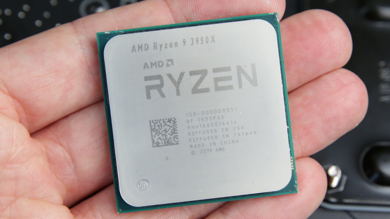
It'll be a nice transition from my aging 3950X tho 😅With 50% more cores and 1.7-1.75x expected better MT it s definitly no, it wont match the Zen/Zen+ to Zen 2 transition.
AMD Ryzen 9 3950X im Test: Benchmarks in Anwendungen und Spielen
AMD Ryzen 9 3950X im Test: Benchmarks in Anwendungen und Spielen / Benchmarks in Anwendungen / Benchmarks in Spielen (Full HD und UHD)www.computerbase.de
Why not? Why does this make any sense at all?SP5 Turin Classic has no successor.
128 cores of Zen 6c will be faster than 128 cores of Zen 5 full? Please explain why.I think that people are failing to see the big change for this generation and not seeing where it will make the most difference. The "c" core CCD is rumored to have the same total amount of L3 cache as the normal core CCD. It's still less per core, but the total local pool is much larger. In addition, with the node improvement, even if just from N3, you still get a notable improvement in throughput per watt. I suspect that, in many cases, 128 cores of Zen 6c will be faster than regular Zen5, and I don't think that there will be a notable difference in all core steady state clocks under load with Zen6 possibly doing better.
Who will buy 192 zen 6p ? And any system bottlenecks that make it less cost effective?Why not? Why does this make any sense at all?
If there is some reason it DOES make sense, then why make anything (other than thread ripper) with full Zen 6 cores?
Put another way .....
What applications will run faster on 96 Zen 6 full cores than on 128 full Zen 5 cores?
128 cores of Zen 6c will be faster than 128 cores of Zen 5 full? Please explain why.
Even if the above is true, in workloads where Turin Zen 5 full was used, it is hard to imagine how 96c Zen 6 could perform better than 128c Zen 5.
Who wants it?Why not?
Because.Why does this make any sense at all?
Because enterprise dinosaurs exist.If there is some reason it DOES make sense, then why make anything (other than thread ripper) with full Zen 6 cores?
Anything sensitive to per-thread perf.What applications will run faster on 96 Zen 6 full cores than on 128 full Zen 5 cores?
idk new cores and N2p looks caaaash mang.128 cores of Zen 6c will be faster than 128 cores of Zen 5 full? Please explain why.
Well each core has 50% moar L3 to access if needed, they clock higher and IPC bump, so should be a fair battle. Memory is actually a wash with the clock uplift and MRDIMM.What applications will run faster on 96 Zen 6 full cores than on 128 full Zen 5 cores?
Each core has up to 4x moar L3 if needed, clocks at actual operating power will be similar enough and IPC is better.128 cores of Zen 6c will be faster than 128 cores of Zen 5 full? Please explain why.
Z6 EPYC having only up to 8 CCD's vs 12/16 for Z5 helps a lot with just about everything, along with the upgrade for dense to 4MB L3/core.Even if the above is true, in workloads where Turin Zen 5 full was used, it is hard to imagine how 96c Zen 6 could perform better than 128c Zen 5.
higher.clocks at actual operating power will be similar enough
It's just that the appeal of gigasockets is limited outside of cloud favelas.SP8 is a cheaper platform than SP5 with a different customer mix, it doesn't have to beat the old all classic part in socket perf, just single core for those who license such things.
Not surprising at all, I wonder how close it is to 9575F clocks.higher.
It's really really funny given what A0 booted at.
Wait, so what is 3D core then. Any bones to throw to help my thinking?yeah.
oh nooo 3D core is something wayyyyy different. Forget about it for a moment.
MLID said that about zen 7Wait, so what is 3D core then. Any bones to throw to help my thinking?
OK but what is it? Experimenting with chip on chip? Experimenting with making a single chip in layers? HmmmMLID said that about zen 7
The leaker claims that Zen 7 chips will have 2 MB of on-die L2 cache per core alongside 7 MB of L3 per core in the form of V-Cache chiplets. This way, AMD is taking the 3D V-Cache concept that it first introduced with the Ryzen 7 5800X3D and giving each Zen 7 CPU core its own V-Cache, hence the term “3D Core”.OK but what is it? Experimenting with chip on chip? Experimenting with making a single chip in layers? Hmmm

 www.notebookcheck.net
It makes little sense for each core to have a distinct own L3 die. Wouldn't it be simply easier to produce just moving the whole L3 to separate die beneath the compute die? I mean they can tune the layout to ensure that each 7MB segment lands underneath a corresponding core making it tad faster to access but should be easier to produce and ensure that that no additional synchro is needed between smaller L3 dies. It might be I have misread the leak though.The leaker claims that Zen 7 chips will have 2 MB of on-die L2 cache per core alongside 7 MB of L3 per core in the form of V-Cache chiplets. This way, AMD is taking the 3D V-Cache concept that it first introduced with the Ryzen 7 5800X3D and giving each Zen 7 CPU core its own V-Cache, hence the term “3D Core”.
Detailed AMD Zen 7 leak reveals new 3D Core, IPC uplift, release date, and more
After teasing some exciting details about Zen 7's new 3D Core, Moore's Law Is Dead has now revealed a plethora of new details. We now know the Zen 7's proposed CPU core variations, release date, IPC, and more. The leaker has also shared more about the new 3D Core.
Yes, that is precisely what they are doing, marees is confused.Wouldn't it be simply easier to produce just moving the whole L3 to separate die beneath the compute die?
You don't want to do that. You need to access a line in L3 that is not currently in your L2. Which L3 slices do you send a request to? If that line can exist in any L3 slice, you would have to send a message to all of them, this would absolutely destroy power efficiency. The way all Zen L3s work is that line placement in slices only depends on the physical address of that line, so that they are evenly striped across all slices. This + extra tag arrays in each L3 slice that cover any lines currently in L2 caches minimizes coherency traffic and can be made quite fast, as shown by how good the Zen L3 generally is.I mean they can tune the layout to ensure that each 7MB segment lands underneath a corresponding core making it tad faster to access
It should speed up sharing information from other L3s if they work it that way.It makes little sense for each core to have a distinct own L3 die. Wouldn't it be simply easier to produce just moving the whole L3 to separate die beneath the compute die? I mean they can tune the layout to ensure that each 7MB segment lands underneath a corresponding core making it tad faster to access but should be easier to produce and ensure that that no additional synchro is needed between smaller L3 dies. It might be I have misread the leak though.
Here is a video from Dr. Ian Cutress. Monolithic 3D. It's being tested on FGPAs first and then may come to CPUs.Wait, so what is 3D core then. Any bones to throw to help my thinking?
Sure, but that's nothing that we didn't know already from back in October last year.

It makes little sense for each core to have a distinct own L3 die. Wouldn't it be simply easier to produce just moving the whole L3 to separate die beneath the compute die? I mean they can tune the layout to ensure that each 7MB segment lands underneath a corresponding core making it tad faster to access but should be easier to produce and ensure that that no additional synchro is needed between smaller L3 dies. It might be I have misread the leak though.
That is Macro not the bitcell which i was referring to.N2 = 38 Mb/mm²
vs
N3E/N4(x)/N5(x) = 31.8 Mb/mm²


That is Macro not the bitcell which i was referring to.
View attachment 130616
View attachment 130617
View attachment 130618
I think that people are failing to see the big change for this generation and not seeing where it will make the most difference. The "c" core CCD is rumored to have the same total amount of L3 cache as the normal core CCD. It's still less per core, but the total local pool is much larger.
In addition, with the node improvement, even if just from N3, you still get a notable improvement in throughput per watt. I suspect that, in many cases, 128 cores of Zen 6c will be faster than regular Zen5, and I don't think that there will be a notable difference in all core steady state clocks under load with Zen6 possibly doing better.