- Mar 3, 2017
- 1,779
- 6,798
- 136

But not a giant silicon based monolithic interposer. Maybe a giant RDL interposer.MLID said it is a giant interposer.
Also, I don't know if this is true, but AMD may dumped (for now) EFB, for now.
OTOH, AMD's Papermaster mentioned that there may be a future EFB with hybrid bond.
I find Dylan make a mountain out of every mole hill. But MLID is a different league, not only is he barely literate on such matters, he just make things up.Also, I don't know if this is true, but AMD may dumped (for now) EFB, for now.
Maybe the specifics are missing. If we are talking about 2.5D packaging, then RDL fanout package makes more sense if the trace counts are low and no active routing logic needed in between the dies. Giant Si Interposer makes less sense, when EFB is there. For 3D stacking, the base die basically can be an Si interposer with functional logic. But I bet MLID would say I told you so even if he said Si Interposer from the beginning.But not a giant silicon based monolithic interposer. Maybe a giant RDL interposer.
Mark my words: Although it is only my humble opinion, I am dead sure about this.
I find Dylan make a mountain out of every mole hill. But MLID is a different league, not only is he barely literate on such matters, he just make things up.
I always found the assumed different node stacking issue strange. At the interface, where the bond actually happens is where they must match. Why would it matter what the interior logic size was, when it was not directly involved? Validation would take time, but the possibility of stacking different nodes appears perfectly normal.On Mi300, MLID has been very good.
Also, another thing that MLID was the first to say is that V-Cache on Zen 4 will be N6. Which the guy from Tom's hardware let slip out yesterday.
Anyway, this would mean that TSMC can stack N5 on N6 (Mi300) and N6 on N5 (Zen 4)
Drive currents, voltage ranges, CTEs etc differs, so they need to take care of such things.I always found the assumed different node stacking issue strange. At the interface, where the bond actually happens is where they must match. Why would it matter what the interior logic size was, when it was not directly involved? Validation would take time, but the possibility of stacking different nodes appears perfectly normal.
So basically design for it.Drive currents, voltage ranges, CTEs etc differs, so they need to take care of such things.
I couldn't find that on THW - do you have a link? Nevertheless, it is quite likely that even THW are sometimes echoing things, MLID mentions.On Mi300, MLID has been very good.
Also, another thing that MLID was the first to say is that V-Cache on Zen 4 will be N6. Which the guy from Tom's hardware let slip out yesterday.
Anyway, this would mean that TSMC can stack N5 on N6 (Mi300) and N6 on N5 (Zen 4)
I couldn't find that on THW - do you have a link? Nevertheless, it is quite likely that even THW are sometimes echoing things, MLID mentions.
A lot of different stuff has been invented to avoid using a giant silicon interposer so I don't know if I believe that it is a single piece of silicon, if that is what they are trying to say. I would definitely doubt that it is a single, monolithic, silicon interposer under all 4 groups of chiplets. It is much more plausible that it is a separate interposer under each set of 2 gpu chiplets (4 silicon interposers total), but even that seems like more than necessary.MLID said it is a giant interposer.
Also, I don't know if this is true, but AMD may dumped (for now) EFB, for now.
OTOH, AMD's Papermaster mentioned that there may be a future EFB with hybrid bond.

I agree with you that this is all highly confusing. AFAIK the Fan-out used on N31 is more or less identical to InFo-R(DL). The Redistribution layer is not silicon based and has no real reticle limit but might be bound to the reticle limit in the certain way, that no single connection can exceed it. The same goes for EFB. As per my understanding the reticle limit there applies to each single bridge, while the composition as a whole is more or less unlimited. Of course I might be terribly wrong.A lot of different stuff has been invented to avoid using a giant silicon interposer so I don't know if I believe that it is a single piece of silicon, if that is what they are trying to say. I would definitely doubt that it is a single, monolithic, silicon interposer under all 4 groups of chiplets. It is much more plausible that it is a separate interposer under each set of 2 gpu chiplets (4 silicon interposers total), but even that seems like more than necessary.
Note that much of the advanced packaging technology has reticle size limits. Even if they are talking about a reticle size limit, that doesn't mean that it is a single, monolithic piece of silicon. It seems more likely to be some form of LSI (local silicon interconnect) and RDL, which can use very thin pieces of silicon embedded under the the die. TSMC has a bunch of different forms of this which all have reticle size limits, although they are likely at 3 or 4x now. I believe the thin peices of silicon can be just passive interconnect or active chiplets, so it seems plausible that they could use an MCD type chiplet under the compute die.
This old link is still a good overview: https://www.anandtech.com/show/16051/3dfabric-the-home-for-tsmc-2-5d-and-3d-stacking-roadmap
None of these use a full silicon interposer. I don't know if the infinity fabric fan-out that they are using for RDNA3 with MCD matches any of these, so that may be something new. I thought they indicated that it was not embedded silicon. I believe they said something about it being derived from tech originally meant for mobile use.
The last slide from the link above looks a lot like the "EFB" that AMD has talked about. It appears to have copper pillars (TIV) that elevate the main chip and allow other chiplets to be embedded underneath. It also shows an SoIC stacked die (like an MCD with v-cache) under other chiplets.
View attachment 76032
A lot of different stuff has been invented to avoid using a giant silicon interposer so I don't know if I believe that it is a single piece of silicon, if that is what they are trying to say. I would definitely doubt that it is a single, monolithic, silicon interposer under all 4 groups of chiplets. It is much more plausible that it is a separate interposer under each set of 2 gpu chiplets (4 silicon interposers total), but even that seems like more than necessary.

Note that much of the advanced packaging technology has reticle size limits. Even if they are talking about a reticle size limit, that doesn't mean that it is a single, monolithic piece of silicon. It seems more likely to be some form of LSI (local silicon interconnect) and RDL, which can use very thin pieces of silicon embedded under the the die. TSMC has a bunch of different forms of this which all have reticle size limits, although they are likely at 3 or 4x now. I believe the thin peices of silicon can be just passive interconnect or active chiplets, so it seems plausible that they could use an MCD type chiplet under the compute die.
This old link is still a good overview: https://www.anandtech.com/show/16051/3dfabric-the-home-for-tsmc-2-5d-and-3d-stacking-roadmap
None of these use a full silicon interposer. I don't know if the infinity fabric fan-out that they are using for RDNA3 with MCD matches any of these, so that may be something new. I thought they indicated that it was not embedded silicon. I believe they said something about it being derived from tech originally meant for mobile use.
The last slide from the link above looks a lot like the "EFB" that AMD has talked about. It appears to have copper pillars (TIV) that elevate the main chip and allow other chiplets to be embedded underneath. It also shows an SoIC stacked die (like an MCD with v-cache) under other chiplets.
View attachment 76032
Not for a single moment do I believe that AMD might produce a silicon interposer north of 1600mm2 - I do not even know if someone in the world is able to do this. And more importantly: There is absolutely no need.No, that his the "base die" - a N6 based die that will have I/O, memory controller, SRAM. There are 4 of them, and each one is 300-350mm2.
Here is a picture from MLID that makes it clearer:
View attachment 76039
The silicon interposer is underneath all of these stacked dies, these being:
- 8x stacks of HBM
- 4x of base die with compute stacked on top of these.
As far as the connections in the picture above, each of the 4 pair of HBM memory most likely only needs to talk to their adjacent base die.
So, one way to save on the size of the silicon interposer would be to have 4 or those connections using different technology.
But the 4 base dies need to have a high bandwidth, low latency interconnect, so possibly the silicon interposer would only be under those 4 base dies.
Intel is using EMIB in SPR to connect the "tiles", but I think the bandwidth requirements of the disaggregated GPGPU is an order of magnitude (or more) higher bandwidth than what SPR requires.
BTW, this may mean nothing, just a rumor, but there is a rumor out there that AMD had yield issues with EFB of the Mi250.
Not for a single moment do I believe that AMD might produce a silicon interposer north of 1600mm2 - I do not even know if someone in the world is able to do this. And more importantly: There is absolutely no need.
The HBM stacks have the same bandwidth demand as the MCD of N31, where InFo-R is sufficient. Apple has shown, that you can produce chiplet GPUs by connecting them via silicon bridge.


Thanks for posting. I'd say at least the first one is a kind of patent they are applying for in the thousands. The kind of trade-offs involved make it possible that we might never see it in a product.Found an interesting patent from AMD for increasing IPC by concurrently executing both sides of a branch instruction.
ALTERNATE PATH FOR BRANCH PREDICTION REDIRECT
View attachment 76053
They need a good bump size of the register file and the other OoO resources to pull this off.
Reposting earlier patents for increasing decode width and multiple op cache pipelines which did not make it to Zen 4.
Not sure what "Re-pipelined front end and wide issue" is going to be or will include such patents at all but interesting regardless.
PROCESSOR WITH MULTIPLE FETCH AND DECODE PIPELINES
View attachment 76051PROCESSOR WITH MULTIPLE FETCH AND DECODE PIPELINES - ADVANCED MICRO DEVICES, INC.
<div p-id="p-0001">A processor employs a plurality of fetch and decode pipelines by dividing an instruction stream into instruction blocks with identified boundaries. The processor includes a branch pwww.freepatentsonline.com
PROCESSOR WITH MULTIPLE OP CACHE PIPELINES
View attachment 76052PROCESSOR WITH MULTIPLE OP CACHE PIPELINES - ADVANCED MICRO DEVICES, INC.
<div p-id="p-0001">A processor employs a plurality of op cache pipelines to concurrently provide previously decoded operations to a dispatch stage of an instruction pipeline. In response to receiving
Compressing Micro-Operations in Scheduler Entries in a Processor
View attachment 76056
Actually in one embodiment, they said to use the resources which would have been used by SMT, so something they might try but indeed it is just a patent and one off at that. But lets say, disable SMT and get IPC gains, sounds acceptable.Thanks for posting. I'd say at least the first one is a kind of patent they are applying for in the thousands. The kind of trade-offs involved make it possible that we might never see it in a product.
For example, a processor (or processor core) that implements simultaneous multithreading executes a software thread along the main path using a first logical or physical pipeline (or first hardware thread) and the alternate path using a second logical or physical pipeline (or second hardware thread).
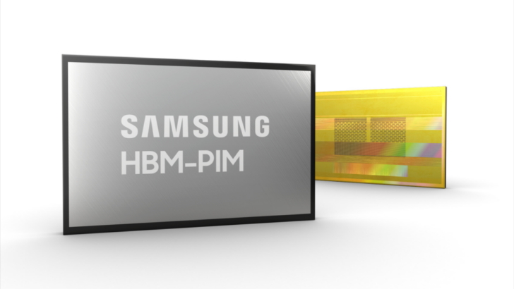
I am wondering if the feature they had with Xilinx Virtex Ultrascale+ with Samsung Aquabolt XL for PIM will make it to Zen 5 DC parts with HBM (MI300 type parts), usually recurring patents and provisional patents are good candidates for making it to a product.PROVIDING ATOMICITY FOR COMPLEX OPERATIONS USING NEAR-MEMORY COMPUTING
From <https://www.freepatentsonline.com/y2022/0413849.html>
APPROACH FOR REDUCING SIDE EFFECTS OF COMPUTATION OFFLOAD TO MEMORY
From <https://www.freepatentsonline.com/y2023/0004491.html>
ERROR CHECKING DATA USED IN OFFLOADED OPERATIONS
From <https://www.freepatentsonline.com/y2022/0318089.html>
DETECTING EXECUTION HAZARDS IN OFFLOADED OPERATIONS
From <https://www.freepatentsonline.com/y2022/0318085.html>
Processing-in-memory concurrent processing system and method
From <https://www.freepatentsonline.com/11468001.html>
OFFLOADING COMPUTATIONS FROM A PROCESSOR TO REMOTE EXECUTION LOGIC
From <https://www.freepatentsonline.com/y2022/0206855.html>
MEMORY ALLOCATION FOR PROCESSING-IN-MEMORY OPERATIONS
From <https://www.freepatentsonline.com/y2021/0303355.html>
Command throughput in PIM-enabled memory using available data bus bandwidth
From <https://www.freepatentsonline.com/11262949.html>
HARDWARE-SOFTWARE COLLABORATIVE ADDRESS MAPPING SCHEME FOR EFFICIENT PROCESSING-IN-MEMORY SYSTEMS
From <https://www.freepatentsonline.com/y2022/0066662.html>
PROCESSOR-GUIDED EXECUTION OF OFFLOADED INSTRUCTIONS USING FIXED FUNCTION OPERATIONS
From <https://www.freepatentsonline.com/y2022/0188117.html>
REUSING REMOTE REGISTERS IN PROCESSING IN MEMORY
From <https://www.freepatentsonline.com/y2022/0206685.html>
PRESERVING MEMORY ORDERING BETWEEN OFFLOADED INSTRUCTIONS AND NON-OFFLOADED INSTRUCTIONS
From <https://www.freepatentsonline.com/y2022/0206817.html>
Providing host-based error detection capabilities in a remote execution device
From <https://www.freepatentsonline.com/11409608.html>
Unless it's a CPU optimized specifically to be the best gaming CPU period.The kind of trade-offs involved make it possible that we might never see it in a product.
Compressing Micro-Operations in Scheduler Entries in a Processor
View attachment 76056

 chipsandcheese.com
Found an interesting patent from AMD for increasing IPC by concurrently executing both sides of a branch instruction.
Exactly this.There has been research/work on this since at least the 90s, and while I believe a few CPUs may do this on an extremely very limited basis (I've seen claims that Apple's big cores can run both paths in certain cases, though that may simply be to allow progress before the branch predictor has its result ready) no one has gone all-in on it because branch predictors are so good these days you won't get much out of it.
Sure, there are some branches that are essentially impossible to predict where it would be of benefit (so long as they aren't quickly followed by more such branches) but then you are paying a price in terms of additional transistors, power to operate them, and verification time for something that doesn't help you very often.
Yeah, MLIDs mock-up is what I meant by "a separate interposer under each set of 2 gpu chiplets (4 silicon interposers total)". That is plausible. Much more plausible than a single giant silicon interposer. You would still need to connect them together somehow, with RDL or embedded bridge chips. The HBM would likely need embedded bridge chips, so you are up to possibly 3 layers of silicon die instead of 2. Four of the "base die" would probably be over 1200 mm2 of silicon with each one not too far from an entire Epyc IO die in size.No, that his the "base die" - a N6 based die that will have I/O, memory controller, SRAM. There are 4 of them, and each one is 300-350mm2.
Here is a picture from MLID that makes it clearer:
View attachment 76039
The silicon interposer is underneath all of these stacked dies, these being:
- 8x stacks of HBM
- 4x of base die with compute stacked on top of these.
As far as the connections in the picture above, each of the 4 pair of HBM memory most likely only needs to talk to their adjacent base die.
So, one way to save on the size of the silicon interposer would be to have 4 or those connections using different technology.
But the 4 base dies need to have a high bandwidth, low latency interconnect, so possibly the silicon interposer would only be under those 4 base dies.
Intel is using EMIB in SPR to connect the "tiles", but I think the bandwidth requirements of the disaggregated GPGPU is an order of magnitude (or more) higher bandwidth than what SPR requires.
BTW, this may mean nothing, just a rumor, but there is a rumor out there that AMD had yield issues with EFB of the Mi250.
If it's nothing new the patent is invalid and completely wasted.It's certainly nothing new, but any company would be foolish to put something in a product that they don't have a patent on. Too many potent trolls out there who are eager for an opportunity for a potential payout.
