Info TOP 20 of the World's Most Powerful CPU Cores - IPC/PPC comparison

Page 5 - Seeking answers? Join the AnandTech community: where nearly half-a-million members share solutions and discuss the latest tech.

Richie Rich

Senior member
Jul 28, 2019
470
229
76
Added cores:
  • A53 - little core used in some low-end smartphones in 8-core config (Snapdragon 450)
  • A55 - used as little core in every modern Android SoC
  • A72 - "high" end Cortex core used in Snapdragon 625 or Raspberry Pi 4
  • A73 - "high" end Cortex core
  • A75 - "high" end Cortex core
  • Bulldozer - infamous AMD core
Geekbench 5.1 PPC chart 6/23/2020:

Pos
Man
CPU
Core
Year
ISA
GB5 Score
GHz
PPC (score/GHz)
Relative to 9900K
Relative to Zen3
1​
Nuvia​
(Est.)​
Phoenix (Est.)​
2021​
ARMv9.0​
2001​
3.00​
667.00​
241.0%​
194.1%​
2​
Apple​
A15 (est.)​
(Est.)​
2021​
ARMv9.0​
1925​
3.00​
641.70​
231.8%​
186.8%​
3​
Apple​
A14 (est.)​
Firestorm​
2020​
ARMv8.6​
1562​
2.80​
558.00​
201.6%​
162.4%​
4​
Apple​
A13​
Lightning​
2019​
ARMv8.4​
1332​
2.65​
502.64​
181.6%​
146.3%​
5​
Apple​
A12​
Vortex​
2018​
ARMv8.3​
1116​
2.53​
441.11​
159.4%​
128.4%​
6​
ARM Cortex​
V1 (est.)​
Zeus​
2020​
ARMv8.6​
1287​
3.00​
428.87​
154.9%​
124.8%​
7​
ARM Cortex​
N2 (est.)​
Perseus​
2021​
ARMv9.0​
1201​
3.00​
400.28​
144.6%​
116.5%​
8​
Apple​
A11​
Monsoon​
2017​
ARMv8.2​
933​
2.39​
390.38​
141.0%​
113.6%​
9​
Intel​
(Est.)​
Golden Cove (Est.)​
2021​
x86-64​
1780​
4.60​
386.98​
139.8%​
112.6%​
10​
ARM Cortex​
X1​
Hera​
2020​
ARMv8.2​
1115​
3.00​
371.69​
134.3%​
108.2%​
11
AMD
5900X (Est.)
Zen 3 (Est.)
2020
x86-64
1683
4.90
343.57
124.1%
100.0%
12​
Apple​
A10​
Hurricane​
2016​
ARMv8.1​
770​
2.34​
329.06​
118.9%​
95.8%​
13​
Intel​
1065G7​
Icelake​
2019​
x86-64​
1252​
3.90​
321.03​
116.0%​
93.4%​
14​
ARM Cortex​
A78​
Hercules​
2020​
ARMv8.2​
918​
3.00​
305.93​
110.5%​
89.0%​
15​
Apple​
A9​
Twister​
2015​
ARMv8.0​
564​
1.85​
304.86​
110.1%​
88.7%​
16
AMD
3950X
Zen 2
2019
x86-64
1317
4.60
286.30
103.4%
83.3%
17​
ARM Cortex​
A77​
Deimos​
2019​
ARMv8.2​
812​
2.84​
285.92​
103.3%​
83.2%​
18​
Intel​
9900K​
Coffee LakeR​
2018​
x86-64​
1384​
5.00​
276.80​
100.0%​
80.6%​
19​
Intel​
10900K​
Comet Lake​
2020​
x86-64​
1465​
5.30​
276.42​
99.9%​
80.5%​
20​
Intel​
6700K​
Skylake​
2015​
x86-64​
1032​
4.00​
258.00​
93.2%​
75.1%​
21​
ARM Cortex​
A76​
Enyo​
2018​
ARMv8.2​
720​
2.84​
253.52​
91.6%​
73.8%​
22​
Intel​
4770K​
Haswell​
2013​
x86-64​
966​
3.90​
247.69​
89.5%​
72.1%​
23​
AMD​
1800X​
Zen 1​
2017​
x86-64​
935​
3.90​
239.74​
86.6%​
69.8%​
24​
Apple​
A13​
Thunder​
2019​
ARMv8.4​
400​
1.73​
231.25​
83.5%​
67.3%​
25​
Apple​
A8​
Typhoon​
2014​
ARMv8.0​
323​
1.40​
230.71​
83.4%​
67.2%​
26​
Intel​
3770K​
Ivy Bridge​
2012​
x86-64​
764​
3.50​
218.29​
78.9%​
63.5%​
27​
Apple​
A7​
Cyclone​
2013​
ARMv8.0​
270​
1.30​
207.69​
75.0%​
60.5%​
28​
Intel​
2700K​
Sandy Bridge​
2011​
x86-64​
723​
3.50​
206.57​
74.6%​
60.1%​
29​
ARM Cortex​
A75​
Prometheus​
2017​
ARMv8.2​
505​
2.80​
180.36​
65.2%​
52.5%​
30​
ARM Cortex​
A73​
Artemis​
2016​
ARMv8.0​
380​
2.45​
155.10​
56.0%​
45.1%​
31​
ARM Cortex​
A72​
Maya​
2015​
ARMv8.0​
259​
1.80​
143.89​
52.0%​
41.9%​
32​
Intel​
E6600​
Core2​
2006​
x86-64​
338​
2.40​
140.83​
50.9%​
41.0%​
33​
AMD​
FX-8350​
BD​
2011​
x86-64​
566​
4.20​
134.76​
48.7%​
39.2%​
34​
AMD​
Phenom 965 BE​
K10.5​
2006​
x86-64​
496​
3.70​
134.05​
48.4%​
39.0%​
35​
ARM Cortex​
A57 (est.)​
Atlas​
0​
ARMv8.0​
222​
1.80​
123.33​
44.6%​
35.9%​
36​
ARM Cortex​
A15 (est.)​
Eagle​
0​
ARMv7 32-bit​
188​
1.80​
104.65​
37.8%​
30.5%​
37​
AMD​
Athlon 64 X2 3800+​
K8​
2005​
x86-64​
207​
2.00​
103.50​
37.4%​
30.1%​
38​
ARM Cortex​
A17 (est.)​
0​
ARMv7 32-bit​
182​
1.80​
100.91​
36.5%​
29.4%​
39​
ARM Cortex​
A55​
Ananke​
2017​
ARMv8.2​
155​
1.60​
96.88​
35.0%​
28.2%​
40​
ARM Cortex​
A53​
Apollo​
2012​
ARMv8.0​
148​
1.80​
82.22​
29.7%​
23.9%​
41​
Intel​
Pentium D​
P4​
2005​
x86-64​
228​
3.40​
67.06​
24.2%​
19.5%​
42​
ARM Cortex​
A7 (est.)​
Kingfisher​
0​
ARMv7 32-bit​
101​
1.80​
56.06​
20.3%​
16.3%​

GB5-PPC-evolution.png

GB5-STperf-evolution.png

TOP10PPC_CPU_frequency_evolution_graph.png


TOP 10 - Performance Per Area comparison at ISO-clock (PPA/GHz)

Copied from locked thread. They try to avoid people to see this comparison how x86 is so bad.[/B]

Pos
Man
CPU
Core
Core Area mm2
Year
ISA
SPEC PPA/Ghz
Relative
1​
ARM Cortex​
A78​
Hercules​
1.33​
2020​
ARMv8​
9.41​
100.0%​
2​
ARM Cortex​
A77​
Deimos​
1.40​
2019​
ARMv8​
8.36​
88.8%​
3​
ARM Cortex​
A76​
Enyo​
1.20​
2018​
ARMv8​
7.82​
83.1%​
4​
ARM Cortex​
X1​
Hera​
2.11​
2020​
ARMv8​
7.24​
76.9%​
5​
Apple​
A12​
Vortex​
4.03​
2018​
ARMv8​
4.44​
47.2%​
6​
Apple​
A13​
Lightning​
4.53​
2019​
ARMv8​
4.40​
46.7%​
7​
AMD​
3950X​
Zen 2​
3.60​
2019​
x86-64​
3.02​
32.1%​


It's impressive how fast are evolving the generic Cortex cores:
  • A72 (2015) which can be found in most SBC has 1/3 of IPC of new Cortex X1 - They trippled IPC in just 5 years.
  • A73 and A75 (2017) which is inside majority of Android smart phones today has 1/2 IPC of new Cortex X1 - They doubled IPC in 3 years.

Comparison how x86 vs. Cortex cores:
  • A75 (2017) compared to Zen1 (2017) is loosing massive -34% PPC to x86. As expected.
  • A77 (2019) compared to Zen2 (2018) closed the gap and is equal in PPC. Surprising. Cortex cores caught x86 cores.
  • X1 (2020) is another +30% IPC over A77. Zen3 need to bring 30% IPC jump to stay on par with X1.

Comparison to Apple cores:
  • AMD's Zen2 core is slower than Apple's A9 from 2015.... so AMD is 4 years behind Apple
  • Intel's Sunny Cove core in Ice Lake is slower than Apple's A10 from 2016... so Intel is 3 years behind Apple
  • Cortex A77 core is slower than Apple's A9 from 2015.... but
  • New Cortex X1 core is slower than Apple's A11 from 2017 so ARM LLC is 3 years behind Apple and getting closer


GeekBench5.1 comparison from 6/22/2020:
  • added Cortex X1 and A78 performance projections from Andrei here
  • 2020 awaiting new Apple A14 Firestorm core and Zen3 core
Updated:


EDIT:
Please note to stop endless discussion about PPC frequency scaling: To have fair and clean comparison I will use only the top (high clocked) version from each core as representation for top performance.
 
Last edited:
  • Like
Reactions: chechito

Doug S

Platinum Member
Feb 8, 2020
2,202
3,405
136
To contrast GB5 with CBR20 (4.4 GHz, 1.344v-1.38v)

CBR20:

ST: ~49W package power
MT: ~162W package power

GB5:

ST: ~42W average, peaked at 46W in Structure from Motion
MT: All over the place, so average seems pointless, but it was ~91W. Ray tracing seemed to push power up to around 142-147W, while Structure from Motion hit the 130s.

Pretty sure Primate Labs claims to use AVX, but . . .


On the ST side the power usage is pretty similar. Cinemark is NOT a general purpose benchmark, it tests only one thing and is pretty meaningless if what you do isn't that one thing or closely related to it. Geekbench and SPEC do a variety of tests to try to form more of an average performance across a variety of tasks. Some things (especially if they have portions that are mostly cache bound so the memory controller isn't exercised as much) will end up using less power than others.

For instance, if you test a database load versus a heavy streaming load (which I assume Cinebench is though I haven't really looked at what it tests because it isn't in the realm of stuff I care about) you will see the database load use a lot less power on a CPU with a lot of cores. It isn't because the database load isn't stressing it, it is because databases can't effectively use all cores all the time due to locking and such. Tasks that are considered "embarrassingly parallel", i.e. those that will benefit from more cores assuming they can get enough memory bandwidth, will burn more and more up to the package max because there are no inter thread depencies.
 
  • Like
Reactions: Richie Rich

Doug S

Platinum Member
Feb 8, 2020
2,202
3,405
136
Anyway, Intel, AMD and IBM's high core count CPUs all have a few things in common; small L1 and L2 caches, and absolutely humongous L3 caches. This is in sharp contrast to the Apple A series which has a huge L1 and L2 cache, with no L3 cache.

You're making an incorrect assumption here. There is nothing stopping a high core count CPU from having huge L1 and L2 caches. The cost of doing so is a bit of area (which designers have in abundance these days) but it does not limit the number of cores other than at the margins - i.e. if bigger caches make the cores a bit larger maybe you only have room for 25 cores instead of 28 at a given die size.

Smaller caches are actually related much more to higher clock rates - because the larger the cache the slower it is, when measured in absolute time (i.e. ns instead of cycles) You don't care too much about absolute latency though, you care about latency when measured in clock cycles - if your pipeline is such that you have to wait a few cycles extra for every L1 access your core will perform terribly. Thus a smaller cache that is faster in terms of latency measured in clock cycles is kind of forced on you if your design targets a high clock rate.

Everything is a tradeoff in CPU design. If you clock faster then you can get twice as much work done versus a core that's clocked half as fast, at least when you don't have to wait on memory or branches or whatever - but clocking higher means all levels of cache and memory are further away in terms of clock cycles so you have to adjust for that with smaller caches with fewer ways. If you go wider, you can get more work done per cycle, at least when your code allows you to fill all the slots, but a wider design burns more power and is more difficult to clock as high.

There isn't one "right" way to do it, different teams choose different points on the high clock / moderate clock and wide / not as wide spectrum, along with many other decisions they have to make. But just about every decision you make implies tradeoffs in other stuff like cache sizing, number of register ports, TLB size and on and on. About the only thing we know for sure that's "wrong" is pursuing clock rate above everything else. That was Intel's goal with the P4 when they talked about hitting 10 GHz eventually. Those 'half cycle' instructions pointed to a pipeline that was 'double pumped' internally. Their goal was to expose that so the half clock becomes a full clock and the clock rate doubles. Unfortunately they found that such a high clock rate burned an unacceptably high amount of power.
 

Carfax83

Diamond Member
Nov 1, 2010
6,841
1,536
136
You're making an incorrect assumption here. There is nothing stopping a high core count CPU from having huge L1 and L2 caches.

Except die space and power limits. From what I understand, SRAM takes up a lot of die space because it's not very dense and it also burns a lot of power because it's often running at the same frequency as the core.

Smaller caches are actually related much more to higher clock rates - because the larger the cache the slower it is, when measured in absolute time (i.e. ns instead of cycles) You don't care too much about absolute latency though, you care about latency when measured in clock cycles - if your pipeline is such that you have to wait a few cycles extra for every L1 access your core will perform terribly. Thus a smaller cache that is faster in terms of latency measured in clock cycles is kind of forced on you if your design targets a high clock rate.

Agreed, which is why Intel, AMD and IBM prefer to have a much larger L3 cache for their multicore CPUs as that lowers latency for the entire CPU while keeping power and thermal within a reasonable state, compared to if they increased the size of the L1 and L2 caches. And this also why a theoretical A13 scaled to 8 big cores would not have 64MB of L2 cache, or even 32MB.

Apple's methodology only makes sense for small core count CPUs that will be doing predominantly single threaded workloads.

If you go wider, you can get more work done per cycle, at least when your code allows you to fill all the slots, but a wider design burns more power and is more difficult to clock as high.

Which is why I am very eager to see how a very wide CPU with relatively low clock speeds like the Apple A series compares to a traditional x86 design across a wide variety of workloads.
 

Doug S

Platinum Member
Feb 8, 2020
2,202
3,405
136
Except die space and power limits. From what I understand, SRAM takes up a lot of die space because it's not very dense and it also burns a lot of power because it's often running at the same frequency as the core.


Your understanding is exactly backwards. Cache is much more dense than random logic. A new process is often first with SRAM since that's the simplest and most dense structure. When Intel claims it has x density for a process their numbers are based on a die of pure SRAM. The power a cache uses it proportional to its clock rate and the type of transistor used, not its size, so going from say 64K to 128K L1 doesn't really use more power other than the leakage current present in any active transistors unless you added more ways of associativity when you increased its size.

L1 is the least dense and L3 the most dense, because L1 is more complex (more ways, more ports etc.) and uses the fastest possible transistors - which implies less density - however even L1 is quite a bit denser than logic blocks like an ALU. L3 is the densest because its as simple as possible and the fastest transistors aren't used because area and power are more important than speed.

Which is why it is really stupid to compare chips in terms of density as I see done here too often (not saying you do it, but those who do know who they are) A wider design with more ALUs will be less dense, a design with bigger cache will more dense, and modern chips have all sorts of other structures like memory controllers, GPUs, NPUs, IPUs and whatever else - I don't know enough about their properties to know the typical relative density of say a memory controller or an NPU but safe to say in a modern SoC like the A13 the CPU cores and caches are such a small part of the overall die that comparing its density to something else made on the same process like HiSilicon's SoC, let alone something made on a totally different process like an Intel CPU is a fool's errand. You might as well compare a Mustang and a Corvette based on how their exhaust smells.
 

DrMrLordX

Lifer
Apr 27, 2000
21,582
10,785
136
I'm looking forward to seeing Apple duke it out with Intel and AMD in anything but Geekbench and Spec2006.

Same. Based on how my Snapdragon 855+ handled the limited Java benchmarking I threw at it (Java adaptation of part of Dr. Cutress' 3DPM), it looked really strong. Kicked the crap out of my old A10-7700k. And we know that Apple has stronger cores than A76. That wasn't even a workload that mobile CPUs "should be good at", and yet, there it was.

On the ST side the power usage is pretty similar. Cinemark is NOT a general purpose benchmark, it tests only one thing and is pretty meaningless if what you do isn't that one thing or closely related to it.

Therein lies the problem. What do you use to gauge IPC? GB5 is more like Antutu in that it is at least partially a user-experience benchmark. Do we regularly rate a CPU's performance based on how quickly it loads a PDF? Normally, no. Geekbench does, and it's a part of the score. I'm reluctant to take any benchmark suite seriously if it includes too many tests that leave execution resources unutilized.
 

Richie Rich

Senior member
Jul 28, 2019
470
229
76
Which is why I am very eager to see how a very wide CPU with relatively low clock speeds like the Apple A series compares to a traditional x86 design across a wide variety of workloads.
@Doug S gave you the example from past about P4. This was exactly same situation -
  • year 2000 - narrow 2xALU P4 core with higher clocks VS. 50% wider 3xALU K8 core with lower clocks
  • year 2020 - narrow 4xALU Intel/AMD core with higher clocks VS. 50% wider 6xALU A13 core with lower clocks
Almost exactly identical situation and we all know which approach won. It's even worse situation for x86 now because Apple's A13 is designed with extreme emphasis about power consumption for mobile devices which K8 was not. Intel was lucky that had mobile Pentium M Banias branch so he was able to shift back on track pretty fast. But Intel/AMD they have no similar product and no experience to do that (look how Samsung terribly failed to develop wide core to compete with Apple). And Samsung did that with Bobcat and Jaguar teams they dragged from AMD during BD exodus.

Another bombshell is that Apple is moving whole lineup including Mac Pros with Xeons. This means Apple is working on server grade CPU:
  • A14 is starting mass production now
  • A15 Xeon server grade CPU is about to tape out (or maybe already running samples)

This would explain still ongoing lawsuit against Nuvia server CPU company. Maybe Apple follows Amazon and will create their own cloud HW to save tremendous amount of money. There is huge difference to pay 7500 USD for 64-core EPYC 7742 versus 500 USD for their own 64-core silicon. And double as powerful one.
 
Last edited:

lobz

Platinum Member
Feb 10, 2017
2,057
2,856
136
OK this is enough for me. Reading through these 5 threads with the same message from Richie Rich but with different titles has been such an excruciating chore, that he managed to turn one of my favorite topics into a PTSD trigger. Good luck to everyone else.
 

Doug S

Platinum Member
Feb 8, 2020
2,202
3,405
136
Therein lies the problem. What do you use to gauge IPC? GB5 is more like Antutu in that it is at least partially a user-experience benchmark. Do we regularly rate a CPU's performance based on how quickly it loads a PDF? Normally, no. Geekbench does, and it's a part of the score. I'm reluctant to take any benchmark suite seriously if it includes too many tests that leave execution resources unutilized.

You don't. IPC is mostly meaningless, because people care about actual performance not performance per clock. Far too much attention is paid to it on these forums.

Personally when I look at a benchmark suite like Geekbench or SPEC I pretty much only look at the compiler benchmark (gcc, clang, llvm whatever) That's impossible to game with compiler tricks and will have a lot of impossible to predict branches, so there has never been a CPU that performs well compiling code that that doesn't perform well on all general purpose code. If a CPU falls short on that benchmark you know it has a glass jaw somewhere. You won't know exactly what but you'll know it has one and can't be trusted for general purpose performance even if it performs terrific on some more narrowly focused benchmark.

If you care about stuff like file compression or whatever exactly Cinemark is measuring then look at the components which do stuff like that, or use a narrow benchmark like Cinemark itself. Just because a benchmark suite like Geekbench has tests that are irrelevant to you doesn't mean the whole thing is irrelevant. The purpose for measuring how long it takes to open a PDF isn't because that is in and of itself important, but because a PDF/PS interpreter is a good proxy for a lot of applications that have to parse a complex file format. Excel will do something similar when you load a complex spreadsheet, a CAD program when you load your design and so on.

Tests aren't irrelevant simply because they don't use all execution resources. A lot of what you do doesn't use all execution resources. You want to see poor execution unit usage and terrible real world IPC look at the trace of a CPU running Oracle sometime. It can't come close to one instruction per cycle on any CPU, despite companies like IBM and Intel investing billions in trying to make it go faster, because the market for hardware that runs databases better is worth billions. If you look at execution unit usage you would say a database is not a worthy benchmark, when for a lot of the market it is the ONLY benchmark that matters.
 

Carfax83

Diamond Member
Nov 1, 2010
6,841
1,536
136
Your understanding is exactly backwards. Cache is much more dense than random logic. A new process is often first with SRAM since that's the simplest and most dense structure. When Intel claims it has x density for a process their numbers are based on a die of pure SRAM. The power a cache uses it proportional to its clock rate and the type of transistor used, not its size, so going from say 64K to 128K L1 doesn't really use more power other than the leakage current present in any active transistors unless you added more ways of associativity when you increased its size.

I guess I should have been more specific. By density I mean the density/capacity ratio. You can fit less of it in a given area because four to six transistors (typically) are required per bit whereas DRAM as a comparison, requires just one transistor per bit.

At any rate, I think my point still stands. A CPU can be optimized to favor single threaded workloads and/or multithreaded workloads by nature of its cache hierarchy. Currently, Apple has optimized their CPUs for single threaded workloads for obvious reasons, while Intel and AMD prefer a more balanced approach as they have greater platform diversity. Of course things will likely change in the future, as Apple starts to target other platforms as well.
 

Carfax83

Diamond Member
Nov 1, 2010
6,841
1,536
136
Almost exactly identical situation and we all know which approach won. It's even worse situation for x86 now because Apple's A13 is designed with extreme emphasis about power consumption for mobile devices which K8 was not. Intel was lucky that had mobile Pentium M Banias branch so he was able to shift back on track pretty fast. But Intel/AMD they have no similar product and no experience to do that (look how Samsung terribly failed to develop wide core to compete with Apple). And Samsung did that with Bobcat and Jaguar teams they dragged from AMD during BD exodus.

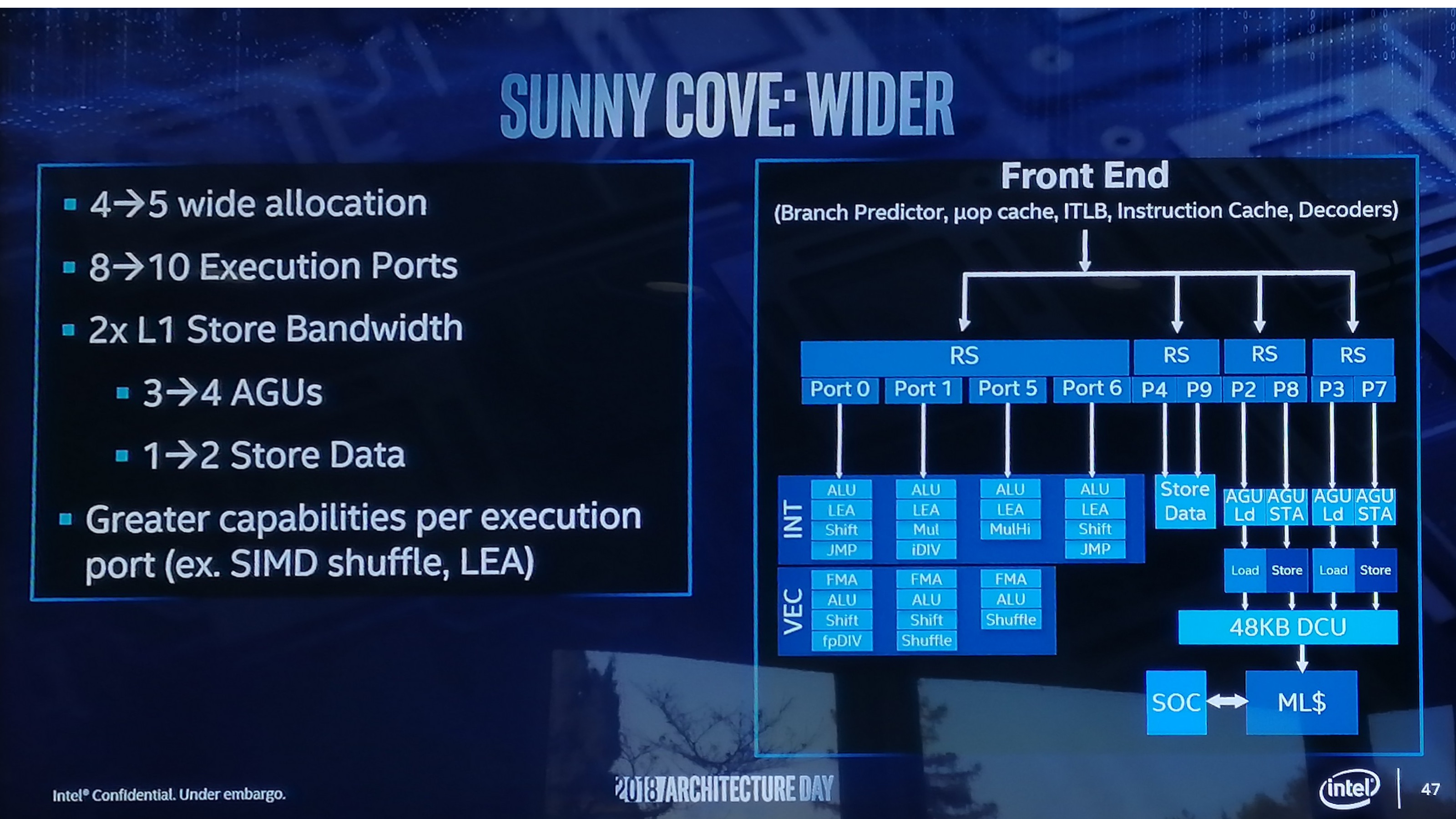
This only holds true because Intel lost so much time with that 10nm fiasco, and AMD were way behind Intel in terms of IPC until Zen. Now both companies are hell bent on making wider designs. Sunny Cove according to Intel is a 5 wide design, and Golden Cove will likely be even wider:

Ronak28.jpg
 

Attachments

  • 1593412252780.png
    1593412252780.png
    7.2 MB · Views: 2

Richie Rich

Senior member
Jul 28, 2019
470
229
76
@Carfax83 Sunny Cove core is not that great in compare to new ARM cores.


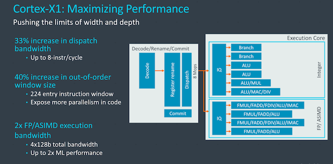
Number of ports:
  • ARM Apple A13 .... 11 wide
  • ARM Cortex X1 ..... 15 wide
  • x86 Sunny Cove .... 10 wide
  • x86 Zen2 ............... 11 wide


ALU comparison:
  • ARM Apple A13 .... 6xALU (2xBranch shared)
  • ARM Cortex X1 ..... 4xALU + 2xBranch in separated ports
  • x86 Sunny Cove .... 4xALU (2xBranch shared, also shared with 3xFPU)
  • x86 Zen2 ............... 4xALU (2xBranch shared)

You can see Intel and AMD has a narrower/weaker design here. ARMs are leaders, especially Apple's design, with its first 6xALU core on the world. No wonder Apple has 82% IPC/PPC lead over Intel/AMD cores. Even Cortex X1 has 40% higher IPC/PPC than Zen2. Those are huge numbers.


AGU comparison:
  • ARM Apple A13 .... 2xAGU (load & store)
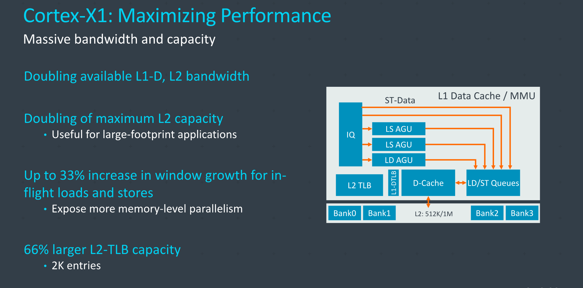
  • ARM Cortex X1 ..... 2xAGU (load & store) + 1xAGU (load) + 2x Store
  • x86 Sunny Cove .... 4xAGU (2xload + 2xstore) + 2x Store
  • x86 Zen2 ............... 2xAGU (load & store) + 1x Store

Looks like Sunny Cove is winner here but it's very store oriented (it has only 2x Load AGU) which means it's built for SIMD operation. Usually 40% of instructions are Load ones so for high IPC in general code there is a winner Cortex X1 with its 3xLoad AGUs. AFAIK it's first core in ther world with 3x Load AGUs. Big question mark is about Apple's AGUs because it looks like the poorest design here. There must be something we don't know IMO.

FPU comparison:
  • ARM Apple A13 .... 3xFPU 128-bit
  • ARM Cortex X1 ..... 4xFPU 128-bit
  • x86 Sunny Cove .... 3xFPU 256(?)-bit
  • x86 Zen2 ............... 2xFPU 256-bit (in 4xpipes)

FPU is the good part of current x86 designs however ARMs did huge improvement and matched that. Don't forget next year new SIMD instruction set SVE2 is coming and it will be another huge step up. The new ARM Fujitsu A64FX with its 2x512-bit SVE SIMD/FPU is beating super computers based on GPU Volta. And SVE2 is designed for 2048-bit so in theory next year can appear ARM cores with a massive 2048-bit FPUs. It isn't about ISA limits anymore. ARM cores can adopt as wide vectors as they need. Such a wide SIMD doesn't make sense for smartphones due to power consumption of course. However what about next gen A64FX? Do you think Fujitsu is sitting still now and enjoys the fame? I expect A64FX-2 is under development and if Fujitsu will keep conservative 2 years cycle we can expect A64FX-2 next year (maybe with 2x1024-bit FPUs).

A78-X1-crop-23_575px.png

A78-X1-crop-24.png


Funny is that weak A76 in Graviton2 (A76 is 3xALU+1xbranch, 2xAGU, 2xFPU only) is beating Zen1 servers very bad and delivers higher performance per thread than Zen2 Epyc Rome systems. And now Cortex X1 has 60% higher IPC than poor A76. Imagine the damage it is gonna make to x86 server systems.
 
  • Haha
Reactions: Tlh97

Doug S

Platinum Member
Feb 8, 2020
2,202
3,405
136
At any rate, I think my point still stands. A CPU can be optimized to favor single threaded workloads and/or multithreaded workloads by nature of its cache hierarchy. Currently, Apple has optimized their CPUs for single threaded workloads for obvious reasons, while Intel and AMD prefer a more balanced approach as they have greater platform diversity. Of course things will likely change in the future, as Apple starts to target other platforms as well.

No, it doesn't. Apple's cache hierarchy is not "optimized to favor single threaded workloads". That same cache hierarchy would work just as well for multi-threaded workloads. The fact Apple doesn't post huge numbers in multithreaded workloads has only to do with the fact that Apple has not designed (or at least has not publicly released) anything with dozens of cores. Intel and AMD have not chosen a "more balanced approach", they simple made a different choice than Apple's designers did.

You are taking the conclusion you want to reach as a given and making up a reason to justify it.
 

JoeRambo

Golden Member
Jun 13, 2013
1,814
2,105
136
The fact Apple doesn't post huge numbers in multithreaded workloads has only to do with the fact that Apple has not designed (or at least has not publicly released) anything with dozens of cores.

I think that's where the question "can they add dozens of cores while keeping same cache hierachy" lies.

Remember good old Core2, that competed with K8 that had IMC, by virtue of having a blob of 4MB of fast L2? Apple has something like that right now, very optimized for clock speed and core number cache hierarchy.

They will need to make tradeoffs if they want to increase clocks ( like keeping same latency in ns, but more from CPU PoV in cycles ). Or once they add more cores, they will need interconnects ( be it rings, crossbars or whatever ), partitioning cache into segments (think Skylake-X with 1MB of L2, or AMD's CCX). And then things like maintaining coherency etc start to bite when no longer have you have blob of fast cache to deal with it, but need to send said traffic to the other side of your chip or to memory.

But one thing is obviuos, Apple has team and resources to pull whatever they want.
 

TheGiant

Senior member
Jun 12, 2017
748
353
106
I think that's where the question "can they add dozens of cores while keeping same cache hierachy" lies.

Remember good old Core2, that competed with K8 that had IMC, by virtue of having a blob of 4MB of fast L2? Apple has something like that right now, very optimized for clock speed and core number cache hierarchy.

They will need to make tradeoffs if they want to increase clocks ( like keeping same latency in ns, but more from CPU PoV in cycles ). Or once they add more cores, they will need interconnects ( be it rings, crossbars or whatever ), partitioning cache into segments (think Skylake-X with 1MB of L2, or AMD's CCX). And then things like maintaining coherency etc start to bite when no longer have you have blob of fast cache to deal with it, but need to send said traffic to the other side of your chip or to memory.

But one thing is obviuos, Apple has team and resources to pull whatever they want.
QFT
I have little doubts performance is there for the A series but as I understand Apple uses very low latency caches
but if they can keep the 8large8small cores concept with reasonable low L2 latency as monolithic this will be a monster
 

Richie Rich

Senior member
Jul 28, 2019
470
229
76
They will need to make tradeoffs if they want to increase clocks ( like keeping same latency in ns, but more from CPU PoV in cycles ). Or once they add more cores, they will need interconnects ( be it rings, crossbars or whatever ), partitioning cache into segments (think Skylake-X with 1MB of L2, or AMD's CCX). And then things like maintaining coherency etc start to bite when no longer have you have blob of fast cache to deal with it, but need to send said traffic to the other side of your chip or to memory.

But one thing is obviuos, Apple has team and resources to pull whatever they want.
Yeah, if you read carefully Andrei's article (HERE) about A13 you will find out that Apple has the best cache subsystem in the game. They have the best engineers so I's easy for them to develop server grade subsystem to scale the high core count efficiently up. Look at Graviton2 based on Neoverse N1 as a first tryout by ARM LLC - it's beating Zen1 and in many ways Zen2 systems. If ARM LLC was able to do that, you can bett Apple can do that with left hand.
 

Doug S

Platinum Member
Feb 8, 2020
2,202
3,405
136
I think that's where the question "can they add dozens of cores while keeping same cache hierachy" lies.

Remember good old Core2, that competed with K8 that had IMC, by virtue of having a blob of 4MB of fast L2? Apple has something like that right now, very optimized for clock speed and core number cache hierarchy.

They will need to make tradeoffs if they want to increase clocks ( like keeping same latency in ns, but more from CPU PoV in cycles ). Or once they add more cores, they will need interconnects ( be it rings, crossbars or whatever ), partitioning cache into segments (think Skylake-X with 1MB of L2, or AMD's CCX). And then things like maintaining coherency etc start to bite when no longer have you have blob of fast cache to deal with it, but need to send said traffic to the other side of your chip or to memory.

But one thing is obviuos, Apple has team and resources to pull whatever they want.


You aren't comparing like for like. Core 2 had an L1 in each core and an L2 shared by the two cores. Skylake had an L1 and L2 in each core, and an L3 shared by the cores. So going from Core 2 to Skylake Intel ADDED per core cache by giving each core its own L2, and made L3 the cache level shared by all. The latter is like Apple, and why Apple will not need to change anything about their L1 and L2 sizes to increase the number of cores, though that doesn't preclude them making such a decision for other reasons - but it won't be simply about increasing the number of cores. There's absolutely nothing stopping them from making a 32 core Mac Pro beast that has the same L1/L2 cache size as found in the iPhone 11's SoC. Or hell, even bigger caches if that's what they think is the best way forward.

Yes you are correct that if they want to increase clocks to any great extent they will either need to accept a latency increase in their caches or reduce their size/complexity to reduce their absolute latency to maintain the same per cycle latency. But who says they are going to target Intel/AMD like clocks? They are able to match Intel/AMD CPUs with FAR higher clock rates at 2.6 GHz so they don't need 5 GHz or even 4 GHz. Probably at about 3.1 GHz they are beating the single thread performance of the fastest turbo'ed (but not overclocked) x86 CPUs on the market. And that's easily within reach using TSMC's N5 and a bit of a boost to the power budget above what a phone's form factor will allow.
 

Doug S

Platinum Member
Feb 8, 2020
2,202
3,405
136
QFT
I have little doubts performance is there for the A series but as I understand Apple uses very low latency caches
but if they can keep the 8large8small cores concept with reasonable low L2 latency as monolithic this will be a monster

Apple's "low latency" caches are more a result of their lower clock rate. Cache latency in nanoseconds is pretty much fixed on a certain process once you've made you choices about its size and complexity. Apple's clock rate is half as fast so their cycles are twice as long in nanoseconds. So even though their caches are bigger which makes them slower in absolute time in nanoseconds, they are pretty quick when measured in cycles due to that slower clock.
 
  • Like
Reactions: lightmanek

JoeRambo

Golden Member
Jun 13, 2013
1,814
2,105
136
The latter is like Apple, and why Apple will not need to change anything about their L1 and L2 sizes to increase the number of cores, though that doesn't preclude them making such a decision for other reasons - but it won't be simply about increasing the number of cores. There's absolutely nothing stopping them from making a 32 core Mac Pro beast that has the same L1/L2 cache size as found in the iPhone 11's SoC.


I don't really follow this argument. Even taking a basic look at Apple core die shots, it is quite obviuos that "32 cores" need a quite a redesign. Sure Apple could in theory duplicate 16 clusters of 2 big cores + big core L2, then proceed to connect said clusters with 16 links to System Agent + System Cache (L3ish), but that is where the problems start with coherency, tags, extra latencies and so on. It would be a challenge to physically fit things and to logically connect them.

Looking at things like Graviton2 from Amazon, reveal that realities of ARM server CPU are unlike those 2 core clusters with uber fast and large L2. And more like mesh network ala Skylake-X, with reduced L2 size from what Apple client CPUs have right now.
 

Doug S

Platinum Member
Feb 8, 2020
2,202
3,405
136
I don't really follow this argument. Even taking a basic look at Apple core die shots, it is quite obviuos that "32 cores" need a quite a redesign. Sure Apple could in theory duplicate 16 clusters of 2 big cores + big core L2, then proceed to connect said clusters with 16 links to System Agent + System Cache (L3ish), but that is where the problems start with coherency, tags, extra latencies and so on. It would be a challenge to physically fit things and to logically connect them.

Looking at things like Graviton2 from Amazon, reveal that realities of ARM server CPU are unlike those 2 core clusters with uber fast and large L2. And more like mesh network ala Skylake-X, with reduced L2 size from what Apple client CPUs have right now.


I'm not claiming you can cut and paste additional cores in, but adding cores is a pretty well understand problem. The hard part is going from one to two, once you've accomplished that adding a third or a 33rd core is a lot easier.

Whether your L2 is 512K or 16MB you still have to connect it to L3 and main memory, handle snooping, coherency and all that fun stuff. It isn't going to be any more of a challenge to "fit things" other than size. i.e. if the overall core is 25% larger due to a bigger L2 then you have room for fewer cores on a die at a given die size target. The fabric and its connectivity takes up the same amount of space regardless of L2 size.

Graviton2's design isn't telling you "this is the only way things can be done" so Apple has to do it like this if they want more cores. It is telling you the decision Amazon's team made. Almost 30 years ago HP designed their PA-RISC chips for servers and workstations with 1MB of L1I and 2MB of L1D. So large for the technology of the time that their caches were off-chip. Only when they went 64 bit in the mid 90s (and Moore's Law caught up to their designs) were they able to move those massive caches on chip. If everyone only solved problems by watching what others do and assuming that's the only way to solve it, there would never be any progress.
 

name99

Senior member
Sep 11, 2010
404
303
136
I don't really follow this argument. Even taking a basic look at Apple core die shots, it is quite obviuos that "32 cores" need a quite a redesign. Sure Apple could in theory duplicate 16 clusters of 2 big cores + big core L2, then proceed to connect said clusters with 16 links to System Agent + System Cache (L3ish), but that is where the problems start with coherency, tags, extra latencies and so on. It would be a challenge to physically fit things and to logically connect them.

Looking at things like Graviton2 from Amazon, reveal that realities of ARM server CPU are unlike those 2 core clusters with uber fast and large L2. And more like mesh network ala Skylake-X, with reduced L2 size from what Apple client CPUs have right now.

No-one is claiming that you would cut and past the iPhone SoC design into a 32 core design!
The claims are that
- sizewise it's hardly outrageous. An Apple large core (A13) is about 4.5mm^2, the L2 is about 4.5mm^2. Group together 4 cores with an L2 and 23mm^2. 8 of those and around 170mm^2. Hardly outrageous. Of course you need some L3, you need memory controllers. But the point is, we're still well within the limits of "easy" areas, not up at 600..800mm^2 difficult areas.
It's pointless investigating the issue further than these rough numbers because we have zero idea what Apple's plans are for how they will handle many core machines.
+ a 16+16 core baseline and dual socket?
+ chiplets?
+ IO/memory/L3 (or L4) on a separate chiplet?
+ GPU as a separate chiplet? Or distributed as slices across each compute chiplet? Or a separate chip (but perhaps mounted on the same package as the compute die?)

- why are you so convinced that designing a NoC and L3 that can scale to many core is a task that's beyond Apple's capabilities? Marvell can do it, Ampere can do it, Amazon can do it -- but somehow when Apple tackles this problem will fall on its face?
How does this assumption make sense?
 

Doug S

Platinum Member
Feb 8, 2020
2,202
3,405
136
- why are you so convinced that designing a NoC and L3 that can scale to many core is a task that's beyond Apple's capabilities? Marvell can do it, Ampere can do it, Amazon can do it -- but somehow when Apple tackles this problem will fall on its face?
How does this assumption make sense?

I don't think people are arguing Apple will fall on its face, they just want to believe that in order to go many core that Apple will have to make changes (like reducing cache size) that will reduce single thread performance. Its the only way they can preserve their belief that Apple is somehow "cheating" with their overly high (when compared to Intel & AMD) single thread results.

First it was because GB/SPEC were somehow tilted in Apple's or ARM's favor, now it is because Apple has very large caches which they want to believe is only possible because Apple SoCs have far fewer cores than the biggest Intel/AMD CPUs . It doesn't make sense, but they have to keep scrambling for some excuse to hold onto because the alternative would be to accept that Macs just might beat Intel & AMD PCs in BOTH single and multi thread performance in a couple years.
 

Carfax83

Diamond Member
Nov 1, 2010
6,841
1,536
136
You can see Intel and AMD has a narrower/weaker design here. ARMs are leaders, especially Apple's design, with its first 6xALU core on the world. No wonder Apple has 82% IPC/PPC lead over Intel/AMD cores. Even Cortex X1 has 40% higher IPC/PPC than Zen2. Those are huge numbers.

You keep forgetting that clock frequency is the other half of the equation for CPU performance. Intel and AMD obviously see the value in designing a more balanced architecture than just focusing on width like the ARM CPUs do.
 

Carfax83

Diamond Member
Nov 1, 2010
6,841
1,536
136
Intel and AMD have not chosen a "more balanced approach", they simple made a different choice than Apple's designers did.

Serious question. Do you know of a single high core count CPU (8 cores and greater) that has had a massive L2 cache attached to it without a L3?

As I said before, I'm not a chip architect and I don't even work in the tech industry. But I follow the industry fairly closely and I can't recall a single high core count CPU using that cache hierarchy.

You are taking the conclusion you want to reach as a given and making up a reason to justify it.

Just because something is possible, doesn't mean it makes sense or should be done. I don't doubt that a high core count CPU with an enormous L2 cache and no L3 could be designed, but would it be as effective as the multilevel cache systems that Intel, AMD and IBM use?

I don't think so.
 
  • Like
Reactions: myocardia

Carfax83

Diamond Member
Nov 1, 2010
6,841
1,536
136
They are able to match Intel/AMD CPUs with FAR higher clock rates at 2.6 GHz so they don't need 5 GHz or even 4 GHz. Probably at about 3.1 GHz they are beating the single thread performance of the fastest turbo'ed (but not overclocked) x86 CPUs on the market. And that's easily within reach using TSMC's N5 and a bit of a boost to the power budget above what a phone's form factor will allow.

I agree, but it must be said that Intel's failed 10nm process didn't do x86 any favors. If Intel had been successful with 10nm, one might wonder whether we would even be having this conversation.