Discussion Speculation: Zen 4 (EPYC 4 "Genoa", Ryzen 7000, etc.)

Page 103 - Seeking answers? Join the AnandTech community: where nearly half-a-million members share solutions and discuss the latest tech.

Vattila

Senior member
Oct 22, 2004
799
1,351
136
Except for the details about the improvements in the microarchitecture, we now know pretty well what to expect with Zen 3.

The leaked presentation by AMD Senior Manager Martin Hilgeman shows that EPYC 3 "Milan" will, as promised and expected, reuse the current platform (SP3), and the system architecture and packaging looks to be the same, with the same 9-die chiplet design and the same maximum core and thread-count (no SMT-4, contrary to rumour). The biggest change revealed so far is the enlargement of the compute complex from 4 cores to 8 cores, all sharing a larger L3 cache ("32+ MB", likely to double to 64 MB, I think).

Hilgeman's slides did also show that EPYC 4 "Genoa" is in the definition phase (or was at the time of the presentation in September, at least), and will come with a new platform (SP5), with new memory support (likely DDR5).

Untitled2.png


What else do you think we will see with Zen 4? PCI-Express 5 support? Increased core-count? 4-way SMT? New packaging (interposer, 2.5D, 3D)? Integrated memory on package (HBM)?

Vote in the poll and share your thoughts! :)
 
Last edited:
  • Like
Reactions: richardllewis_01

jpiniero

Lifer
Oct 1, 2010
14,510
5,159
136
There is certainly the potential to feed more bandwidth into the core with DDR5 and AVX-512 execution units would definitely eat that up. It will be interesting to see how DDR5 will affect various applications and games, in light of the longer latency.

JEDEC vs JEDEC, the latency increase isn't that much. The people complaining about the DDR5 latency are comparing JEDEC to XMP (which I doubt it used in servers).
 

Thibsie

Senior member
Apr 25, 2017
727
752
136
Rumours pointed to Zen5 being (with many other things) a hybrid core, one Zen4 core and one Zen5 core with shared registers.
I dunno anything about the possibility of this but I'm very curious though.
 

DisEnchantment

Golden Member
Mar 3, 2017
1,590
5,722
136
Regardless of whether Zen4 is just a redesigned core or not, with L3 being same and a confirmed die size of 72.226mm2 on N5P, Zen4 core will pack anything between 25-40% more transistors
[If we assume horrible scaling, e.g. 70% of the Zen3 core will scale a measly 1.1x, while the 30% scale at 1.5x (vs TSMC's advertised 1.8x)]
All the new interconnect logic is in the cIOD, CXL, GenZ ,MPDMA, NVDIM/SCM etc., sot they dont contribute to the CCD die area.
Zen4 is far from being an optical shrink for sure.

Zen3 core over Zen2 core is just ~9% increase within similar power envelope.
Looking at the chart below, N7 -->N5P [23%perf/-49%power reduction].
If AMD keeps same clocks, the efficiency gain is enormous.


1635278170930.png
 

maddie

Diamond Member
Jul 18, 2010
4,723
4,628
136
Regardless of whether Zen4 is just a redesigned core or not, with L3 being same and a confirmed die size of 72.226mm2 on N5P, Zen4 core will pack anything between 25-40% more transistors
[If we assume horrible scaling, e.g. 70% of the Zen3 core will scale a measly 1.1x, while the 30% scale at 1.5x (vs TSMC's advertised 1.8x)]
All the new interconnect logic is in the cIOD, CXL, GenZ ,MPDMA, NVDIM/SCM etc., sot they dont contribute to the CCD die area.
Zen4 is far from being an optical shrink for sure.

Zen3 core over Zen2 core is just ~9% increase within similar power envelope.
Looking at the chart below, N7 -->N5P [23%perf/-49%power reduction].
If AMD keeps same clocks, the efficiency gain is enormous.


View attachment 51936
Minor correction. I think it's really a 40% power reduction in total if following the specs.
 

Saylick

Diamond Member
Sep 10, 2012
3,084
6,184
136
I must have missed something. It's confirmed to be N5P not vanilla N5?
AMD haven't come out to say what version of N5 they will use, but the rumors have said that they will be using an enhanced version or something along those lines. It could be N5P or something more specific for AMD.


Saylick

Diamond Member
Sep 10, 2012
3,084
6,184
136

NostaSeronx

Diamond Member
Sep 18, 2011
3,683
1,218
136
Now I know who is the right person to ask about K9 (it wasn't Jim!).
K9 was Mitch Alsup -> 65nm 5 GHz Opteron
K10 was Charles R. Moore -> 45nm Bulldozer
//Specifically, the two closest to release versions. With Alsup's K9 taping out then being canned, and Moore's K10 being shown on roadmaps then canned.

Greyhound = 10h, since at that point they stopped publicizing Kx names.

2005/2007 being two keypoints of K9's development guesstimated by AMD in 2003:
amdk9.png
-> The Sunnyvale, Calif.-based company is "working like crazy" on the K9, an underlying architecture, or blueprint, for a new generation of chips, said Fred Weber, chief technology officer of AMD's computational products group, during an interview at the Microprocessor Forum here Wednesday.
-> Chips based on the K9 architecture will likely be released--at least in sample quantities--by the second half of 2005, Weber said.
-> "We will have a multicore product," Weber said.
Which coincides with the above by AMD's FW.

K9's Trace Cache location:
k9-k10.png
 
Last edited:

jamescox

Senior member
Nov 11, 2009
637
1,103
136
@moinmoin
I think we can all agree that going back monolith is not THE solution. Chiplets have clear benefits and are the way to go. Now there are taxes because of the Interconnect. The IOD needs that much power because it needs to drive all those bits via the interconnect.
With the current Interconnect via organic package you need around 15pJ/bit of energy. With something like EMIB or Info-LSI you only need 1-2pJ/bit. So this way of packaging is clearly a way to go. And the competitor we dare not to name will clearly use such a solution on order to scale its newly announced SoC to 2x and 4x.

I believe the original ISSCC paper on the zeppelin die from 2018 said 11 pJ/bit for IFIS and 2 pJ/bit for IFOP. This doesn’t seem to jive with your numbers; where are they from? The IFOP can be highly optimized since they run on package with a maximum distance of 1 to 2 cm. I would expect the power to have increased, but the speed has also increased significantly so it is unclear where the current power per bit will be. If the original IFOP was 2 pJ/bit, I would expect a silicon bridge to be significantly lower than that.

Connecting the cpu die with silicon bridges is problematic. They can’t do long runs so the die have to be placed directly adjacent. This might work for 4 or 6 dies but would be difficult for 8 or more. The current packages route the serdes links for the outer chips under the inner chips. To use embedded silicon bridges, it seems like they would need to daisy chain them. That isn’t necessarily a bad solution. It would just be an extra hop across a silicon bridge, but you would need to route across an entire die. It seems like it would be better to stack die in that case. Extreme core count processors are generally lower clock anyway.

I have wondered if they would make a modular IO die such that multiple smaller IO die could be used for Epyc. That might allow some other options like mounting the cpu die close the IO die with silicon bridges and distributing the IO die with serdes connections. Later they could move to a stacked solution with embedded silicon interconnect between IO die. It seems more like the standard Zen4 Epyc might be very conservative such that it is very similar to current Epyc processors. We might get a less conservative (more stacking) version of Zen 4 later leading to a zen 5 stacked version.
 

BorisTheBlade82

Senior member
May 1, 2020
660
1,003
106
@jamescox
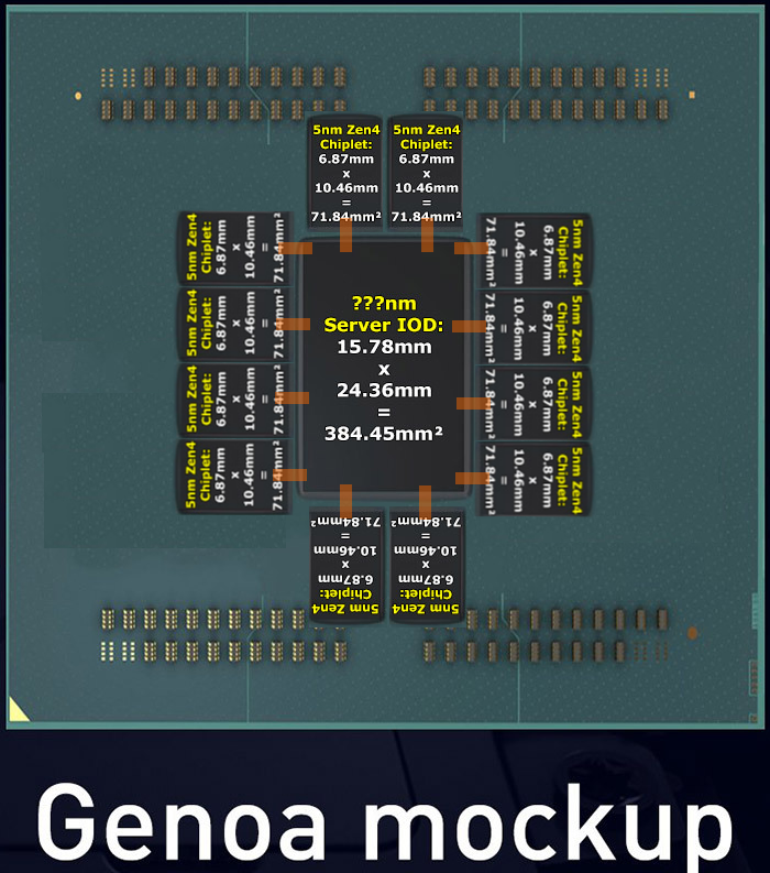
As it happens some months ago I made a mockup of how EPYC Genoa could look like with silicon die Interconnects. I know that this is more wishful thinking than anything else.
Zen-4-Info-LSI-Mockup.png


To your question about the numbers. These are really hard to come by and I just realized that I remembered them totally wrong. From what I gathered some time ago was next to your numbers: 1-2 pj/bit for IFOP, 0,1-0,2 for EMIB/CoWoS etc. and as a really rough estimate around 0,05-0,1 for 5mm on-die.
The point still is that advanced packaging saves around 10x interconnect consumption and diminishes the advantage of a monolith by a huge amount.


As to your suggestion with modular IODs. That sounds quite interesting as well. This is a topic where a lot of developments can be imagined - especially with the lack of expert knowledge I have 😉
 
  • Like
Reactions: Tlh97

Ajay

Lifer
Jan 8, 2001
15,332
7,792
136
Regardless of whether Zen4 is just a redesigned core or not, with L3 being same and a confirmed die size of 72.226mm2 on N5P, Zen4 core will pack anything between 25-40% more transistors

That's a lot more xtors than needed just for the AVX-512 registers, pipelines, etc. Now I'm really curious what's going on. I think those who said this will be like the Zen1 to Zen2 improvement may be correct. There's the usual suspects like op cache, retire buffer, TLBs, etc. But, how about a larger L2? I wish the Zen3 Wikichip page had as much detail as he had for Zen1.

Zen4 is far from being an optical shrink for sure.

Did someone think otherwise?

If AMD keeps same clocks, the efficiency gain is enormous.

Heck, AMD could pip the top clocks by 5% for improved ST and still beat Zen3 on power usage by a good margin (for Raphael at least).


Eh, I'm getting over excited based on a short interview with Mike Clark. Mike deserves a gold star for that interview (and Ian too). Lisa Su must love this guy.
 
  • Like
Reactions: Tlh97

moinmoin

Diamond Member
Jun 1, 2017
4,934
7,619
136
As it happens some months ago I made a mockup of how EPYC Genoa could look like with silicon die Interconnects. I know that this is more wishful thinking than anything else.
Zen-4-Info-LSI-Mockup.png
The problem with this approach is that in the current CCDs the IFOP links are in the center of the die. Will be interesting how links at the edges will behave latency wise with distance being more different between near and far cores. Also if AMD were planning to just place the CCDs along the sides of an IOD they could have chosen to create a far more rectangular aspect ratio for the package to facilitate this. So I expect them to choose some different approaches we may not be thinking of yet.
 

jamescox

Senior member
Nov 11, 2009
637
1,103
136
The problem with this approach is that in the current CCDs the IFOP links are in the center of the die. Will be interesting how links at the edges will behave latency wise with distance being more different between near and far cores. Also if AMD were planning to just place the CCDs along the sides of an IOD they could have chosen to create a far more rectangular aspect ratio for the package to facilitate this. So I expect them to choose some different approaches we may not be thinking of yet.
The IFOP die area was in the middle, between the 2 CCX on Zen 2 but it moved to the edge of the die on Zen 3.
 

moinmoin

Diamond Member
Jun 1, 2017
4,934
7,619
136
The IFOP die area was in the middle, between the 2 CCX on Zen 2 but it moved to the edge of the die on Zen 3.
Duh, you're right indeed (they moved it there to make room for the 3D V-Cache).

Though it's on a long edge not a short one (where it couldn't link directly to the L3$ with the current layout).
 

jamescox

Senior member
Nov 11, 2009
637
1,103
136
That's a lot more xtors than needed just for the AVX-512 registers, pipelines, etc. Now I'm really curious what's going on. I think those who said this will be like the Zen1 to Zen2 improvement may be correct. There's the usual suspects like op cache, retire buffer, TLBs, etc. But, how about a larger L2? I wish the Zen3 Wikichip page had as much detail as he had for Zen1.


Did someone think otherwise?


Heck, AMD could pip the top clocks by 5% for improved ST and still beat Zen3 on power usage by a good margin (for Raphael at least).


Eh, I'm getting over excited based on a short interview with Mike Clark. Mike deserves a gold star for that interview (and Ian too). Lisa Su must love this guy.
I don’t know how reliable the rumors are about L2 cache size increases. The larger vector units might take quite a lot of die area, but I have wondered if they might move to a large, shared L2 similar to Apple designs. A lot of applications really like large, fast L2 cache. That would also allow disabling cores for maximum single core performance. Large L3 cache could be stacked so spending more die area on fast L2 could be a good way to go.
 
  • Like
Reactions: Tlh97

leoneazzurro

Senior member
Jul 26, 2016
905
1,430
136
That's a lot more xtors than needed just for the AVX-512 registers, pipelines, etc. Now I'm really curious what's going on. I think those who said this will be like the Zen1 to Zen2 improvement may be correct. There's the usual suspects like op cache, retire buffer, TLBs, etc. But, how about a larger L2? I wish the Zen3 Wikichip page had as much detail as he had for Zen1.

I think the Gigabyte leaks on AM5 mainboards already revealed that Zen4 will have 1Mbyte of L2 cache.

 
Last edited:

moinmoin

Diamond Member
Jun 1, 2017
4,934
7,619
136
If one looks at the changes in the cores from Zen to Zen 2 and the ones from Zen 2 to 3 one can notice that the latter makes mostly architectural changes while the former does mostly size changes (wider, larger, more, needing more die area). I'm expecting Zen 4 to follow the pattern of the former.

The rhythm seems to be:
- Ground up re-design, same node optimization. (~Zen, Zen 3)
- Same design optimized and extended to make good use of the additional area afforded by new smaller node. (Zen 2, Zen 4?)

That'd make Mike Clark's excitement about Zen 5 understandable as well considering that's the next ground up re-design in the queue, the first with AMD being the healthy company it is nowadays.

Btw.
Mike Clark said:
So every three years, we're pretty much redesigning it all.
New Zen gen only every 18 months confirmed. @DrMrLordX vindicated ;)
(The interview is actually a little fuzzy on that since later on they talk about another three years later being Zen 8, not 7. But that's by Ian and Clark just seems to play along without really confirming or denying it.)
 
Last edited:

jamescox

Senior member
Nov 11, 2009
637
1,103
136
@jamescox
As it happens some months ago I made a mockup of how EPYC Genoa could look like with silicon die Interconnects. I know that this is more wishful thinking than anything else.
Zen-4-Info-LSI-Mockup.png


To your question about the numbers. These are really hard to come by and I just realized that I remembered them totally wrong. From what I gathered some time ago was next to your numbers: 1-2 pj/bit for IFOP, 0,1-0,2 for EMIB/CoWoS etc. and as a really rough estimate around 0,05-0,1 for 5mm on-die.
The point still is that advanced packaging saves around 10x interconnect consumption and diminishes the advantage of a monolith by a huge amount.


As to your suggestion with modular IODs. That sounds quite interesting as well. This is a topic where a lot of developments can be imagined - especially with the lack of expert knowledge I have 😉
The mock-up looks like it would fit better rotated 90 degrees. I am still expecting serdes in the Genoa implementation. I suspect there will be a higher end device that comes a bit later that makes more use of stacking; that might be a 128 core variant. If they do that, it could be essentially a test run for future Zen 5 Epyc. Might only be low volume, very high price, HPC though. There are so many possibilities with stacking that it is very difficult to predict. It sounds like Intel will have an HPC cpu with HBM eventually, so they likely need to use some embedded silicon bridges or interposers with HBM to compete with that. I don’t know if massive, stacked L3 will be sufficient.
 

Ajay

Lifer
Jan 8, 2001
15,332
7,792
136
I think the Gigabyte leaks on AM5 mainboards already revealed that Zen4 will have 1Mbyte of L2 cache.

Ah, good memory. I forgot about that. I was thinking at least double that - though slower, the hit rate would be very high in many workloads because it is inclusive. And it would still be backed by the even larger L3$ victim cache.

I have developed too many other interests to follow CPU and process developments in detail anymore. Still enough interest though to hang around here and annoy people 😈
 

BorisTheBlade82

Senior member
May 1, 2020
660
1,003
106
@jamescox
I am with you. As I said the mockup is more wishful thinking as coincidentally the geometrics would allow it. But yes, AMD will stick to IFOP with Genoa. The trouble is this: I do not think that it is technically possible to use IFOP on one SKU and CoWoS etc. on another SKU with the same CCD. So I guess IFOP will stay with us for another full product stack. So it might very well be that Apple will be first in this area as well.
 

DisEnchantment

Golden Member
Mar 3, 2017
1,590
5,722
136
But yes, AMD will stick to IFOP with Genoa. The trouble is this: I do not think that it is technically possible to use IFOP on one SKU and CoWoS etc. on another SKU with the same CCD. So I guess IFOP will stay with us for another full product stack.
Hmmm ... I dont think that is the route AMD will take with Genoa.

1635412130998.png
Zen4 CCD from the Gigabyte leak likely has two SDP/IF links.
On top of that to support 96 or even 128 cores would mean they need to support up to 512 SerDes links.
Way too much power wasted and looking at the routing for Rome above already is very complicated.
On Rome they had to route the links underneath the CCD.

And in ISSCC 2021, Sam Naffziger already alluded to interposers/higher density interconnects (highlighing by me). This was before Lisa announced 3D V-Cache.
1635413672201.png
In fact from this slide we knew the second item already is coming to Zen3. (Cache while not exactly memory is backed by SRAM which is memory)

From TSMC's offical data, CoWoS-L with LSI/Si bridges is proven and it reaches 3x reticle size which can cover all chiplets for a hypothetical 16 CCD EPYC.
1635412906172.png

Anyway, I think AMD will most likely go with some sort of interposer, probably CoWoS-R if not CoWoS-L if there is really no need for super high density interconnects. i.e. if 4um contact pitch is enough (i.e. CoWoS-R) instead of the high density CoWoS-L (<1um pitch)
If not, they will burn power linking those 96/128 cores, it is not sustainable.
You can read yourself the paper by Naffziger
 
Last edited: