Good catch, I forgot it was in slices, duh. Having to snoop another CCX's L3 through the IOC will be necessary for Rome's cache coherency protocol, so I'd expect it in Matisse as well.Technically it's not 16MB per CCX but 4MB per core. Every core has write access to its own 4MB L3$. Every core has read access to all L3$ of the whole chip. Obviously read access to the 12MB L3$ of the other cores within the same CCX is faster than the L3$ of all the cores on other CCX's.
I believe that even for the two CCX's on the same chiplet the access between them causes a round trip through the IOC. But that will have to be tested once the chips are publicly available.

Speculation: The CCX in Zen 2
Page 14 - Seeking answers? Join the AnandTech community: where nearly half-a-million members share solutions and discuss the latest tech.
You are using an out of date browser. It may not display this or other websites correctly.
You should upgrade or use an alternative browser.
You should upgrade or use an alternative browser.
beginner99
Diamond Member
- Jun 2, 2009
- 5,320
- 1,768
- 136
A "L4$" would only make sense when implemented into the IOC as that would allow saving round trips otherwise necessary to reach other CCX's and as such open up the bandwidth of those IOC to chiplet IF-links for other uses.
To save round trips that l4 would need to be inclusive of all L3 available. It adds up quickly especially on Rome. That would probably only be feasable with edram but that wouldn't be faster than going to other ccx via IO die.
I believe that even for the two CCX's on the same chiplet the access between them causes a round trip through the IOC. But that will have to be tested once the chips are publicly available.
Advantage here would be that a multi-chiplet CPUs perform exactly the same as single-chiplet eg. making performance predictable which is often desired.
Soulkeeper
Diamond Member
- Nov 23, 2001
- 6,740
- 156
- 106
- Oct 22, 2004
- 822
- 1,466
- 136
Wow!
AMD slide showing that Zen 3 EPYC will still be 9 dies, probably with 8 core CCXs.

So no 15 chiplets for EPYC 3, as rumoured by SemiAccurate. That rumour could have referred to later generations on the roadmap, though.
But more interesting to me is that the CCX size goes to 8 cores. In this thread, I've speculated about topologies based on the direct-connected 4-core CCX, and I have suggested that the benefit of direct-connection would mean that the 4-core complex would remain the basic building block. My main argument has been that any topology beyond 4 nodes would have to use a suboptimal scheme compared to direct-connection. However, there are topologies for 8 nodes that can retain the optimal connections within two quad-core groups.
Here are some topologies I proposed for connecting 8 nodes (in the Zen 2 speculation thread here). I drew these way back when we were speculating about the possibility of L4 in the IO chiplet. In this case, the nodes would be the L3 cache slices connected to each core — which I presume is the way they will design it, similar to the 4 slices shared in the current 4-core CCX. Topologies (e-g) retain the optimal connections of cores within each 4-core group.
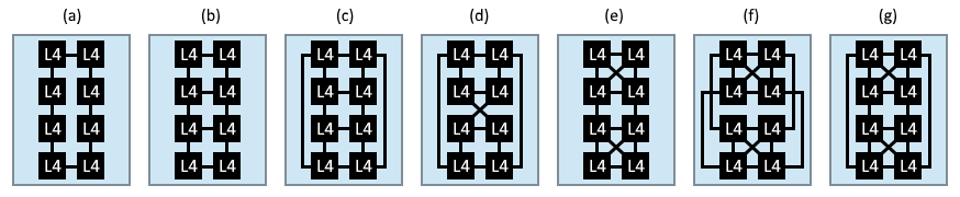
Figures (a-d) are simple textbook topologies; (a) ring, (b) mesh, (c) cube and (d) twisted cube (see Zapetu's suggestion below). Figure (e-g) are variants of mesh and cube topologies, enhanced with direct connections between the nodes in the upper and lower quads: (e) mesh with two fully connected quads, (f) cube with upper and lower sides fully connected, and (g) same cube topology as (f), but with the lower quad flipped vertically.
@Zapetu may have been spot on in his speculation (in this post): "Intel has used many different topologies for their multi-socket servers, but in my opinion, this one looks the best for this kind of situation:"

"You can find the above diagram and more information here. Every processor is 2 hops away from any other processor. By connecting a pair of memory controllers where the IOHs sit, you get quite uniform access to them too. If you are using this topology for the IOD (between L4 slices) then why not use the same topology for the 8-core CCX (between L3 slices)."
AMD slide showing that Zen 3 EPYC will still be 9 dies, probably with 8 core CCXs.
So no 15 chiplets for EPYC 3, as rumoured by SemiAccurate. That rumour could have referred to later generations on the roadmap, though.
But more interesting to me is that the CCX size goes to 8 cores. In this thread, I've speculated about topologies based on the direct-connected 4-core CCX, and I have suggested that the benefit of direct-connection would mean that the 4-core complex would remain the basic building block. My main argument has been that any topology beyond 4 nodes would have to use a suboptimal scheme compared to direct-connection. However, there are topologies for 8 nodes that can retain the optimal connections within two quad-core groups.
Here are some topologies I proposed for connecting 8 nodes (in the Zen 2 speculation thread here). I drew these way back when we were speculating about the possibility of L4 in the IO chiplet. In this case, the nodes would be the L3 cache slices connected to each core — which I presume is the way they will design it, similar to the 4 slices shared in the current 4-core CCX. Topologies (e-g) retain the optimal connections of cores within each 4-core group.
Figures (a-d) are simple textbook topologies; (a) ring, (b) mesh, (c) cube and (d) twisted cube (see Zapetu's suggestion below). Figure (e-g) are variants of mesh and cube topologies, enhanced with direct connections between the nodes in the upper and lower quads: (e) mesh with two fully connected quads, (f) cube with upper and lower sides fully connected, and (g) same cube topology as (f), but with the lower quad flipped vertically.
@Zapetu may have been spot on in his speculation (in this post): "Intel has used many different topologies for their multi-socket servers, but in my opinion, this one looks the best for this kind of situation:"
"You can find the above diagram and more information here. Every processor is 2 hops away from any other processor. By connecting a pair of memory controllers where the IOHs sit, you get quite uniform access to them too. If you are using this topology for the IOD (between L4 slices) then why not use the same topology for the 8-core CCX (between L3 slices)."
DrMrLordX
Lifer
- Apr 27, 2000
- 23,217
- 13,300
- 136
@Vattila
I wouldn't be so sure that Zen3 will have 8c per CCX. We may be looking at 4c CCX with shared L3 instead of seeing L3 married to the CCX. Makes me wonder what the interconnect between CCXs and L3 will be, and how it will affect performance. Currently, on Zen2, it appears that L3 performance is linked to CPU clockspeed; for example, I can lower L3 latency AND memory latency just by increasing the static clockspeed of my 3900x. Will this new L3 run asynchronously from CPU clock? Or will the design require clock synchronization between CCXs?
I wouldn't be so sure that Zen3 will have 8c per CCX. We may be looking at 4c CCX with shared L3 instead of seeing L3 married to the CCX. Makes me wonder what the interconnect between CCXs and L3 will be, and how it will affect performance. Currently, on Zen2, it appears that L3 performance is linked to CPU clockspeed; for example, I can lower L3 latency AND memory latency just by increasing the static clockspeed of my 3900x. Will this new L3 run asynchronously from CPU clock? Or will the design require clock synchronization between CCXs?

- Oct 22, 2004
- 822
- 1,466
- 136
I wouldn't be so sure that Zen3 will have 8c per CCX
If they chose one of topologies (e-g), you basically have two highly connected 4-core CCXs, so in that case I would agree that they still have a 4-core CCX as the basic building block. As far as I understand, currently the two Zen 2 CCXs in a chiplet are only connected via the IO chiplet. With the change to shared L3 in the Zen 3 chiplet, and assuming one of topologies (e-g), the 4-core CCXs will be directly connected through their shared L3, making an 8-core super-CCX.
(Note: Replace L4 by L3 in these diagrams.)
However, it is possible that the topology of the cache slices are so different, for example (a-d), that you no longer have the 4-core building block.
Last edited:
- Oct 22, 2004
- 822
- 1,466
- 136
Currently, on Zen2, it appears that L3 performance is linked to CPU clockspeed
I guess that will remains so. These are low level interconnects between cache slices, just as before.
- Oct 22, 2004
- 822
- 1,466
- 136
What if they made an L3 chiplet? That would be weird.
Discrete L3 wouldn't meet power-efficiency targets, I guess.
nicalandia
Diamond Member
- Jan 10, 2019
- 3,331
- 5,282
- 136
There is laterally no benefits of going beyond 4 core CCX, more Cache? Yes, but more than 4 cores will increase the complexity. Just keep adding more CCDs and the I/O will handle the communications just fine.
- Oct 22, 2004
- 822
- 1,466
- 136
There islaterallyno benefits of going beyond 4 core CCX
Well, some will argue that 8 cores tightly integrated with a shared L3 is an 8-core CCX, but in the end this is just nomenclature, which AMD will decide.
As discussed above, what is apparent, is that there is room for a lot of reuse of the 4-core CCX. Each L3 slice only needs another connection port to connect to the corresponding slice in the other 4-core group.
I presume that the low-level interconnects between cache slices in the 4-core groups and between groups are of the same kind, to optimise uniformity in latency. In other words, I doubt they use two 4-core CCXs with high-level Infinity Fabric routing between them, to link up cache slices. That would have very non-uniform latency, with a cost to average latency. Remember, the CCX uses an interleaved memory scheme, so memory accesses typically hit every L3 slice equally.
Last edited:
That would be more or less in line with the RDNA WGP, which is basically 2 CU's using a shared cache pool.@Vattila
I wouldn't be so sure that Zen3 will have 8c per CCX. We may be looking at 4c CCX with shared L3 instead of seeing L3 married to the CCX. Makes me wonder what the interconnect between CCXs and L3 will be, and how it will affect performance. Currently, on Zen2, it appears that L3 performance is linked to CPU clockspeed; for example, I can lower L3 latency AND memory latency just by increasing the static clockspeed of my 3900x. Will this new L3 run asynchronously from CPU clock? Or will the design require clock synchronization between CCXs?
Not only that, unless you were using a die directly mounted on the logic, the latency would seriously increase (even then it might go up, no idea what stack interconnects introduce to latency equation).Discrete L3 wouldn't meet power-efficiency targets, I guess.
LightningZ71
Platinum Member
- Mar 10, 2017
- 2,691
- 3,390
- 136
We've seen that, with Intel's processors, ring busses are still highly effective out to 8 cores. What's to stop AMD from just moving the CCX to a big, fast ring bus with eight cores in it, an L3 on it, and a link to the IO die at another stop?
moinmoin
Diamond Member
- Jun 1, 2017
- 5,248
- 8,463
- 136
Personally I'd hesitate to conclude on some topology changes based on that one slide (which essentially limits the actually confirmed changes to a plus sign behind the L3$ amount per CCD). My take away is that AMD intends to (finally) tackle the fact that the current L3$ setup with local per-core slices by far doesn't make the best use of the whole amount of L3$ available on each CCD (or package for that matter). I can imagine significant changes to the cache coherency protocol, possibly decentralizing the coherency buffer structure back again from the IOD closer to the CCXs without touching the CCX structure itself.Wow!
AMD slide showing that Zen 3 EPYC will still be 9 dies, probably with 8 core CCXs.
So no 15 chiplets for EPYC 3, as rumoured by SemiAccurate. That rumour could have referred to later generations on the roadmap, though.
But more interesting to me is that the CCX size goes to 8 cores. In this thread, I've speculated about topologies based on the direct-connected 4-core CCX, and I have suggested that the benefit of direct-connection would mean that the 4-core complex would remain the basic building block. My main argument has been that any topology beyond 4 nodes would have to use a suboptimal scheme compared to direct-connection. However, there are topologies for 8 nodes that can retain the optimal connections within two quad-core groups.
Here are some topologies I proposed for connecting 8 nodes (in the Zen 2 speculation thread here). I drew these way back when we were speculating about the possibility of L4 in the IO chiplet. In this case, the nodes would be the L3 cache slices connected to each core — which I presume is the way they will design it, similar to the 4 slices shared in the current 4-core CCX. Topologies (e-g) retain the optimal connections of cores within each 4-core group.
Figures (a-d) are simple textbook topologies; (a) ring, (b) mesh, (c) cube and (d) twisted cube (see Zapetu's suggestion below). Figure (e-g) are variants of mesh and cube topologies, enhanced with direct connections between the nodes in the upper and lower quads: (e) mesh with two fully connected quads, (f) cube with upper and lower sides fully connected, and (g) same cube topology as (f), but with the lower quad flipped vertically.
@Zapetu may have been spot on in his speculation (in this post): "Intel has used many different topologies for their multi-socket servers, but in my opinion, this one looks the best for this kind of situation:"
"You can find the above diagram and more information here. Every processor is 2 hops away from any other processor. By connecting a pair of memory controllers where the IOHs sit, you get quite uniform access to them too. If you are using this topology for the IOD (between L4 slices) then why not use the same topology for the 8-core CCX (between L3 slices)."
Edit: After catching up with all the unread posts from the Zen 3 Speculation thread DisEnchantment's post on patents likely is the best indicator yet what has changed.
Last edited:
- Oct 22, 2004
- 822
- 1,466
- 136
I can imagine significant changes to the cache coherency protocol, possibly decentralizing the coherency buffer structure back again from the IOD closer to the CCXs without touching the CCX structure itself.
Does the IO chiplet currently contain a cache-coherency directory, or is cache-coherence decentralised in the L3 caches?
Does the IO chiplet currently contain a cache-coherency directory, or is cache-coherence decentralised in the L3 caches?
I don't know, it's like that patent is being purposefully ambiguous.
PS. I had some time yesterday and made a drawing of how I think the Zen2 cache hierarchy works. This is just a logical diagram, it's a bit lame, since I haven't used power point in a long time.
moinmoin
Diamond Member
- Jun 1, 2017
- 5,248
- 8,463
- 136
A lot of the uncore is unconfirmed secret sauce unfortunately. I can't find the die shot of the Zen 2 CCD and IOD anymore, but they looked pretty similar to the respective areas on the Zeppelin die. Personally I'd have expected the cache-coherency directory being part of the SCF (scalable control fabric) under control of the ARM core, so part of the uncore respective IOD. But some of the patents do sound like there is no directory yet and the cores are responsible for keeping data coherent themselves.Does the IO chiplet currently contain a cache-coherency directory, or is cache-coherence decentralised in the L3 caches?
DisEnchantment posted another patent. So far to me it looks like this: Zen 2 introduced the TAGE predictor as second layer branch predictor. It works on historic data, the more data the more accurate the prediction. If the predictor can't load from RAM the three local cache levels are the natural limit for the highest possible prediction accuracy. Above patent to me appears to be an approach how to extend it to all data in RAM. @DisEnchantment's previously posted patents...
- essentially applies the TAGE predictor principle to accelerating exchange of data between caches
- make the memory controllers aware of the different levels of predictors and be able to react/prepare accordingly (this appears to assume that TAGE predictors don't work on a per core level but exchange data across the whole package. Since TAGE improves on depth of historic data that should be easier to achieve if such data is shared across the package)
- use the predictor to move data in down time when the core itself is busy
- reduce the amount of data (and as such power used) by preferably sending smaller delta diffs of data
TRENDING THREADS
-
 Discussion Zen 5 Speculation (EPYC Turin and Strix Point/Granite Ridge - Ryzen 9000)
- Started by DisEnchantment
- Replies: 25K
-
Discussion Intel Meteor, Arrow, Lunar & Panther Lakes + WCL Discussion Threads
- Started by Tigerick
- Replies: 24K
-
 Discussion Intel current and future Lakes & Rapids thread
- Started by TheF34RChannel
- Replies: 23K
-

-

AnandTech is part of Future plc, an international media group and leading digital publisher. Visit our corporate site.
© Future Publishing Limited Quay House, The Ambury, Bath BA1 1UA. All rights reserved. England and Wales company registration number 2008885.