Speculation: The CCX in Zen 2

Page 12 - Seeking answers? Join the AnandTech community: where nearly half-a-million members share solutions and discuss the latest tech.

How many cores per CCX in 7nm Zen 2?

  • 4 cores per CCX (3 or more CCXs per die)

    Votes: 55 45.1%
  • 6 cores per CCX (2 or more CCXs per die)

    Votes: 44 36.1%
  • 8 cores per CCX (1 or more CCXs per die)

    Votes: 23 18.9%

  • Total voters
    122

dnavas

Senior member
Feb 25, 2017
355
190
116
5ghz all core 16 cores??..no one ever suggested that did they??
That's certainly been the impression I've been left with.
I'm sure it's just one group going "hey, lots of cores" and another group going "high speed awesome GloFo-ness" and another group going "and more IPC, lower IF latency, and wider vector units". All of these things are not going to come to pass. Not at the same time.
 
  • Like
Reactions: french toast

scannall

Golden Member
Jan 1, 2012
1,944
1,638
136
That's certainly been the impression I've been left with.
I'm sure it's just one group going "hey, lots of cores" and another group going "high speed awesome GloFo-ness" and another group going "and more IPC, lower IF latency, and wider vector units". All of these things are not going to come to pass. Not at the same time.
To be clear. 16 cores at 5 Ghz is a unicorn.Or maybe a male dog that doesn't lick his balls. However, 7nm Global Foundries is an IBM node. And they do know clock speed. 12 cores, and 48 threads at 5.5 Ghz in a shipping product doesn't suck even if it won't play Crysis.

The potential is there, but until parts are actually out the door we won't know what has been realized.
 

AtenRa

Lifer
Feb 2, 2009
14,000
3,357
136
If it is not obvious, try this: Again draw 8 small squares, representing cores, on a paper. Now partition them into two groups of four with a dashed line down the middle. Fully connect the cores in each group (6 links each).

Now you can start experimenting with interconnecting the two groups across the dashed line. Note that at a minimum a single additional link will do. But you will be able to decrease the maximum number of hops between any two cores in separate groups by adding more links. You may add additional intermediate nodes (routers). Draw these as small circles. You are now creating complex topologies (hyper-cube, fat tree, etc.).


8core_CCX.png

Edit 1: You dont need the cross bars, this is a MESH with-in a CCX.
Edit 2: Now I think of it, you dont need a CCX. Connect all cores with IF directly. For the EPYC die this will be much better. You can have a 16 core die and then add 4x dies for a 64 core SKU.

Edit 3: I was thinking something like that for a 16core die for the EPYC CPUs. At 7nm it should be close to 200-220mm2. You can add 4x dies for a single 64core SKU.

8core_die_7nm.png
 
Last edited:

HurleyBird

Platinum Member
Apr 22, 2003
2,670
1,250
136
You'd probably want to space out the memory controllers in order to even out access latency, like Intel does in its mesh interconnect server chips.

But yeah, there are a few different viable topologies. I'd wager on something that works well with a theoretical active interposer based interconnect though, or at least something that isn't worse than the current CCX arrangement.
 
Last edited:

french toast

Senior member
Feb 22, 2017
988
825
136
That's certainly been the impression I've been left with.
I'm sure it's just one group going "hey, lots of cores" and another group going "high speed awesome GloFo-ness" and another group going "and more IPC, lower IF latency, and wider vector units". All of these things are not going to come to pass. Not at the same time.
No chance, for a start I have accepted the fact we will not see 8 core CCX without new topology.

Second; I don't think we will get 16 cores either with 8 core CCX or 4x4..too much die area, amd will want the die to be significantly smaller than summit ridge for obvious reasons.

Thirdly; 16 cores at 5ghz all core turbo? That is plain ridiculous honestly, 105w tdp? Nope not going to happen.
What I think will happen is a 12 core CPU for AM4, either 2x 6 core CCX or 3x 4 core CCX.
This allows for a smaller die and better yeilds, it allows for a escalation of the core wars, it allows for higher all core turbo's (Vs 16 cores@tdp), it keeps the threadripper relevant, it allows for future core wars expansion on AM4.

We could get;
- R7 3700 10 core ~60w for $329........4.5Ghz Single core turbo.
- R7 3700x 10 core ~80w for $399......4.7ghz dual core turbo.
- R7 3800x 12 core ~105w for $499....5.0ghz dual core turbo.

If zen2 can offer 4x 256bit vector and a good 10-15% integer IPC...then the ~60w 3700 10 core would duke it out with a $450 i9 9900k quite comfortably imo.
3800x could be highly binned (top 1-5%) part that is held in reserve for Q3/Q4 for possible sneaky icelake counter.
This launch cycle could continue every year, with x800x SKU launching alongside threadripper XX series.
 

moinmoin

Diamond Member
Jun 1, 2017
4,933
7,619
136
Perhaps I missed it, but has anyone done an analysis of how a "40% performance boost OR 60% total power reduction" is going to yield 16 cores at 5Ghz?
One doesn't have to do anything with the other. The process node characteristics on which stats like "40% performance boost OR 60% total power reduction" are usually based on the most efficient range of the node which for GloFo's 14LPP/12LP stops at around 3.3GHz. Everything above is increasingly inefficient, but AMD, Intel and most of the desktop consumer market don't care in this case. Thus the problem is the frequency hard wall 14LPP/12LP (as an efficiency optimized node, LPP = Low Power Plus) comes with at currently between 4.1-4.3GHz. At that point the increasing inefficiency (and resulting heat) becomes completely unworkable (with standard cooling solutions). Thanks to IBM's involvement so far a lot of us expect GloFo's 7nm based node (to be used for Ryzen 3xxx) to be optimized for high performance instead, meaning the process node characteristics should allow for a more gradual decrease of efficiency (= increase of heat) thus allowing top frequencies higher than the current 4.1-4.3GHz.
 

Vattila

Senior member
Oct 22, 2004
799
1,351
136
[8-core CCX diagram] [16-core die diagram]

I find it very cool that you actual did diagrams — that shows enthusiasm for architecture, and that I like!

Regarding your 8-core CCX — where did the shared L3 go? It is hard to assess how your design would compare to the Zen 4-core CCX without that detail. Your diagram implies that there are two hops between the dual-cores (core-router-core). If you put your shared L3 cache in the router you could alleviate that somewhat, with an architecture similar to the shared L3 cache in the 4-core CCX. It may even be more efficient. That said, this dual-core mini-CCX is a smaller building block than the 4-core CCX, so the efficiency may be lost when you scale up.

Four of your dual-cores are then direct-connected on the next level of scale, introducing another hop in your 8-core CCX. So latency between the dual-cores may be similar or even better than the Zen 4-core CCX, but you give up some of that on average for your 8-core CCX.

Aside: Consider SMT4 instead of your dual-cores for a similar 16-thread building block using the Zen 4-core CCX.

Regarding your 16-core die, this is obviously a server or HEDT design by current standards, so not a scalable design that can span from mobile to server like the Zen CCX architecture can do. For a 16-core die as a building block for MCM or chiplet design, I don't think your diagram and description includes enough information to evaluate it against a 4 x 4-core CCX Zen design. It very much depends on how the cores are wired up, which your diagram does not detail (I presume they are all not connected through a single crossbar, which would not scale well). Maybe some actual chip architects will chime in with an opinion.

One observation though: Your 16-core die design would perform worse, compared to the 4-core CCX Zen design, in some special but important use-cases. In particular, consider virtualisation with a partitioning size of 4 cores per virtual machine.
 

dnavas

Senior member
Feb 25, 2017
355
190
116
One doesn't have to do anything with the other.

We may be in violent agreement with each other.

The process node characteristics ... are usually based on the most efficient range ... which ... stops at around 3.3GHz.

Indeed. I prefer to start based on what we know, or at least what we assume we know from what we're told, which is why I started by talking about the R1700's 8 core, 3Ghz base. For a desktop chip, a 40% improvement means we're looking at ~65W tdp 4.2Ghz base clock, all other things being equal (which they won't be, but that's a starting point). 12 core would be ~100W, which matches nicely to the current 2700X tdp. A 16-core requires another 30W. There's only two ways to ship a 16 core to the desktop, one is to lower the base clocks, like TR2 is doing, the other is to ship a hair dryer. I'm not sure I'd want 130W base-clock chip on AM4. Are there desktop users that would put up with <4Ghz base clocks in exchange for 16 cores? That conclusion is entirely before we get to 1) turbo and 2) overclocking.

If we're lucky, the wall moves up a matching/linear 40%, and we've got headroom to 5.5ish. Aside from assumptions made due to IBM's involvement, we have no evidence that it will, and also precious little evidence that GloFo is even going to be able to deliver 7nm. Which is why I don't understand:

12 cores, and 48 threads at 5.5 Ghz in a shipping product...

Actually, there are a number of things I don't understand in that quote, one of which is 12 cores at 5.5Ghz. If you've got plenty of power delivery, and the wall has moved, you might be able to OC to 5.5Ghz on 12 cores. Maybe. Barely. Like my 1800X does to 4Ghz. (which it doesn't -- not Prime95 stable) I wouldn't bet the farm on it.

The other thing I don't understand -- 48 threads? SMT4? What good is SMT4 on the desktop? It'll only serve to increase average latency and power use (and a headache wrt cache utilization) in the hope of improving throughput on a processor that isn't being tasked that way. In order to have the computational units to adequately use SMT4, you won't be seeing 4.2base / 5.5 turbo. If Zen2 comes with SMT4 (which would make sense for Epyc), it would be the first thing to disable when gaming. If you expect 48 threads to operate similarly to the existing 16 threads on your 8 core processors, you need three times the active units. I would expect a lot closer to R1700 clocks on such a processor as 3x power requirements entirely absorbs the benefits of 7nm. There's no additional clocking room. I don't see that happening on desktop. Sure, it's lovely to play a numbers/quantity game, but it makes very little sense. Unless AMD really isn't going to pursue frequency on the desktop. I would be disappointed by that outcome.

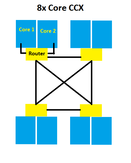
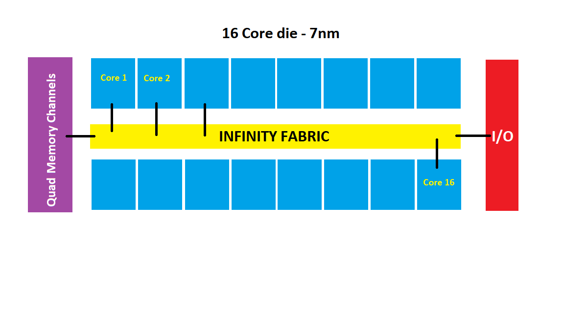
I haven't read the semiaccurate post which likely gives some insight into the coming Epyc chips, but one way to account for the hype of what is public is to postulate a 6 core base CCX with SMT4 (or a triple quad-core-CCX die). 192 threads would be monstrous on a server. The thing is, I'm not sure that would carry over to the desktop. Whether you spin it as "desktop-oriented CCX", or you just leave the extra units unpowered, I expect that any throughput-oriented optimizations for Epyc won't be carried over to the desktop. One of the more persuasive arguments for keeping the 4-core CCX and delivering a quad-CCX die for Epyc and a triple-CCX die for desktop is specifically because of the different scaling you get from tdp and frequency scaling. It allows you to have a basic core which you lay out in two different manners for server and desktop. SMT4 is a good counter-argument for leaving the die of both at 12 cores (while disabling it on desktop). I'm sure we'll know in 6 months. I'm happy to be wrong about any and all of this :shrug:
 

maddie

Diamond Member
Jul 18, 2010
4,723
4,628
136
It has been indicated that Zen1 and Zen2 teams started work simultaneously. I have to assume that once the Zen1 team was finished on the 1st iteration of Zen then they began work on Zen3. If we can take this as a reasonable assumption, then Zen2 shares most of the Zen1 layout with the added tuning that was unable to be done for a 2017 release.

Once we can accept this, then all of the extreme speculation disappears as being unreasonable. Zen2 will almost certainly mirror Zen1 closely in layout, as the foundational work was shared, and the additional Zen2 work related to optimizations of a server product and a desktop one. They most probably will be fabbed separately anyhow.

With a few more highly likely assumptions about 7nm and cores/CPU, we can get a fair a idea as to what is Zen2.

Anyhow, this is my reasoning.
 

Vattila

Senior member
Oct 22, 2004
799
1,351
136
It has been a long time since I started this thread, and with AMD's Horizon event upcoming in one week (Nov 6) — presumably giving a lot of details about Zen/EPYC 2, and finally answering the question about the CCX core-count — it is soon time to lay it to rest.

Curiously, with exactly 100 votes, the poll today stands at 47% votes for 6-core, 46% for 4-core and 7% for 8-core. With the persistent rumour that EPYC 2 will be a 64-core 8+1 chiplet design, a 6-core CCX is highly unlikely, and an 8-core CCX is now more likely. Feel free to change your vote.

Will it be 4-core or 8-core?
 

Gideon

Golden Member
Nov 27, 2007
1,608
3,573
136
It has been a long time since I started this thread, and with AMD's Horizon event upcoming in one week (Nov 6) — presumably giving a lot of details about Zen/EPYC 2, and finally answering the question about the CCX core-count — it is soon time to lay it to rest.

Curiously, with exactly 100 votes, the poll today stands at 47% votes for 6-core, 46% for 4-core and 7% for 8-core. With the persistent rumour that EPYC 2 will be a 64-core 8+1 chiplet design, a 6-core CCX is highly unlikely, and an 8-core CCX is now more likely. Feel free to change your vote.

Will it be 4-core or 8-core?
Regardless of the CCX type, I really hope the cores are still packed further away from each other like with the current config in quads. Having 8 cores side-by-side will get really hot with high clocks @7nm. And even if it's still 4 core CCX, i hope the huge 32MB L3 cache is now at least somewhat unified between the two CCXes in the chiplet ( perhaps the extra 16MB part?)
 
May 11, 2008
19,300
1,129
126
What makes me wonder, is that the CCX as a 4 core unit, needs a fast ports between each CCX.
Let say that AMD makes the data fabric ports between the CCX 2x as wide for 7nm zen 2.
It makes me wonder if AMD could update the CCX in the sense that a wider data fabric would be useful.
To prevent any bottle necks somewhere else and maximum use.
 

beginner99

Diamond Member
Jun 2, 2009
5,208
1,580
136
It has been a long time since I started this thread, and with AMD's Horizon event upcoming in one week (Nov 6) — presumably giving a lot of details about Zen/EPYC 2, and finally answering the question about the CCX core-count — it is soon time to lay it to rest.

Curiously, with exactly 100 votes, the poll today stands at 47% votes for 6-core, 46% for 4-core and 7% for 8-core. With the persistent rumour that EPYC 2 will be a 64-core 8+1 chiplet design, a 6-core CCX is highly unlikely, and an 8-core CCX is now more likely. Feel free to change your vote.

Will it be 4-core or 8-core?

Well the actually options say 4-core ccx with 3 ccx per die which is also makes no sense with 8 + 1. I still changed my vote to that but I expect same as zeppelin 2x4-core ccx per die. Albeit of course the cores are overworked and also the cache and the ccx interconnect improved. I suspect that would be less work than a going with a 8-core die with a ringbus.
 
  • Like
Reactions: Vattila

DisEnchantment

Golden Member
Mar 3, 2017
1,590
5,722
136
Speculating here, not really skilled in this art
The present invention may be better understood, and its numerous objects, features, and advantages made apparent to those skilled in the art by referencing the accompanying drawings.

From the rumors flying around and what I can dig up from the patents I come up with this. I just copied the patent drawings :)
I hope sources of CPC, S|A, David Schor, (AdoredTV) etc are not Patent analysers rather real industry scouts
G6sok0O.png

- 8 Core CCX (Also mentioned by S|A, patent drawings indicate so but it is exemplary)
- Single L3 in one CCX (from #20180239708, #20180143829, #20180165202) same as Zen 1
- Memory Controller located in another chiplet connected by an interconnect (called bridge chiplet by AMD) (from #20180239708, #20180143829, #20180165202)
- Data compression across IF (from Patents see #20180167082 (across sockets) and #20180052631 (across dies)) not in Zen 1. If compressed data is lesser than bus width the extra bits are not even signalled. (#20180314655)
- Directory Controller for L3 sync across dies ( from Patents see #20180239708) which is not the case in Zen 1
- According to David Schor/gcc patches Load/Store costs for(>=256 bit SSE) are halved. I don't know if it is definitive but this is a significant improvement.
- Many improvements related to cache if Patents are to be believed. Something like 8-10 patents in last year.
- Wider??? hopefully
- I heard NUMA only across sockets not within a node.


But if AMD New Horizon is any indication we will hear about these in the AMD Next Horizon in a couple of days.
Hopefully I get at least some of these points right :D


I came across this

I have seen so many recent AMD patents covered by this DoE Contract of a mere 32 Million USD.


*Many of the Patents are still not awarded
 
Last edited:

Glo.

Diamond Member
Apr 25, 2015
5,658
4,417
136
Nobody has spotted that AMD essentialy quadrupled the L3 cache size, on CCX, and double CCX size?
 

JoeRambo

Golden Member
Jun 13, 2013
1,814
2,105
136
Nobody has spotted that AMD essentialy quadrupled the L3 cache size, on CCX, and double CCX size?

We did, and it gives great hopes. Flat 8C CCX backed by 32MB of hopefully fast L3 is a match in heaven for Ryzen core.

But too early to get excited, as Ryzen disclosures had 16MB of L3, that eventually turned into 8MB of usable L3 for each CCX and caching scheme was rather not optimal.
 

krumme

Diamond Member
Oct 9, 2009
5,952
1,585
136
We did, and it gives great hopes. Flat 8C CCX backed by 32MB of hopefully fast L3 is a match in heaven for Ryzen core.

But too early to get excited, as Ryzen disclosures had 16MB of L3, that eventually turned into 8MB of usable L3 for each CCX and caching scheme was rather not optimal.
Yeaa the devil is in the detail. How fast is the cache is what matters. So we are left with hope atm.

Now even if it's fast cache it's probably also a sign the core is slim and not beefed up.
Can't get it all. So it's a trade-off anyways.

I also wonder if the consoles need more wide fpu than what is in Zen and have the mm2 budget for it?

Makes sense to make a slim high freq Zen 2 for it all and beef it up in Zen 3.

My hope goes especially towards a high freq node. We really need that too.
 

HurleyBird

Platinum Member
Apr 22, 2003
2,670
1,250
136
I also wonder if the consoles need more wide fpu than what is in Zen?

If anything, they could probably make do with less given how power constrained they are and how things are evolving with GPU compute already.
 

beginner99

Diamond Member
Jun 2, 2009
5,208
1,580
136
I also wonder if the consoles need more wide fpu than what is in Zen and have the mm2 budget for it?
Who says consoles will use zen2? They can just use zen1. Which makes more sense anyways since Zen1 already exists on 14/12nm and I doubt consoles will start on 7nm. Too expensive.
 

HurleyBird

Platinum Member
Apr 22, 2003
2,670
1,250
136
Who says consoles will use zen2? They can just use zen1. Which makes more sense anyways since Zen1 already exists on 14/12nm and I doubt consoles will start on 7nm. Too expensive.

They'll probably be on 7nm because they're still some ways off, they need to make a tangible leap over the mid-gen refreshes, and if one manufacturer uses on an older node while the other one doesn't, they most likely lose that generation.
 

Tuna-Fish

Golden Member
Mar 4, 2011
1,324
1,462
136
Just to throw some gasoline on the flames: The first Linux kernel patches for Zen2 support are in. The interesting part is that it was not sufficient just to add the definitions for Zen2, but they also had to change how the lookup happens a little, because the PCI root topology of the Zen2 core differs from Zen1. That patch set can not really be used as proof for a specific system configuration, only that it's different from what there used to be.
 

yuri69

Senior member
Jul 16, 2013
373
573
136
Just to throw some gasoline on the flames: The first Linux kernel patches for Zen2 support are in. The interesting part is that it was not sufficient just to add the definitions for Zen2, but they also had to change how the lookup happens a little, because the PCI root topology of the Zen2 core differs from Zen1. That patch set can not really be used as proof for a specific system configuration, only that it's different from what there used to be.
It seems, the Data Fabrics of dies in a CPU are connected through CAKE but now they also expose their PCI root complexes. Is this plausible?
 
Mar 11, 2004
23,031
5,495
146
Who says consoles will use zen2? They can just use zen1. Which makes more sense anyways since Zen1 already exists on 14/12nm and I doubt consoles will start on 7nm. Too expensive.

I think they'll be 7nm because they'll be using GPUs that were engineered for 7nm. I don't see them trying to backport that to older processes. Now, maybe they'll split them and use a 12nm Zen+ design paired with 7nm GPU, but I think it'll be best to offer one chip as it'll help overall packaging, plus the CPU part probably won't be too big, and it being 7nm will help keep the overall power of the system lower. I suppose it might would be possible for them to go with two 7nm chips as a way to keep costs down (versus a single larger custom chip). So they go with a mid-range Zen 2 consumer chip - think 2600, and a mid-range GPU - think RX x70 level, which means they'd be using off the shelf parts that AMD sells in consumer PC space so no custom chip.

7nm is expensive but they'll likely be on 7nm for awhile so they'll make up for it in volume and can stick with the hardware longer (vs doing "Slim" versions). And the density and power savings likely has other benefits for them. 7nm should enable them to offer substantial performance improvements over the PS4 Pro/One X, while using similar power and thermal systems. If they go with 12nm they'll have to beef up the power and thermal designs of the consoles, and even then there will be limits to what they can offer as far as increases in performance.

They'll probably be on 7nm because they're still some ways off, they need to make a tangible leap over the mid-gen refreshes, and if one manufacturer uses on an older node while the other one doesn't, they most likely lose that generation.

PS5 is likely late next year or early 2020, and the next Xbox is 2020, they're not that far off. I agree that they'll need 7nm to offer much over the One X/PS4 Pro. Plus, we know that Navi was designed for 7nm, and it was built with Sony/PS5 in mind, and it should be out first. And with it due likely late 2020, the next Xbox is almost certainly 7nm.
 

beginner99

Diamond Member
Jun 2, 2009
5,208
1,580
136
If they go with 12nm they'll have to beef up the power and thermal designs of the consoles, and even then there will be limits to what they can offer as far as increases in performance.

4 Zen1 cores will obliterate 8 jaguar cores easily especially in single-threaded limited scenarios. clock them at their optimum around 2.5 ghz and they are very power efficient. I admit the gpu part would be somewhat of an issue. Vega 56-like could be around 450mm2 + 96mm2 for 4 zen1 cores = 550mm2 on 14nm. maybe bit smaller on 12nm. For sure doable in 2020 when yields should be excellent.