A few stupid questions:
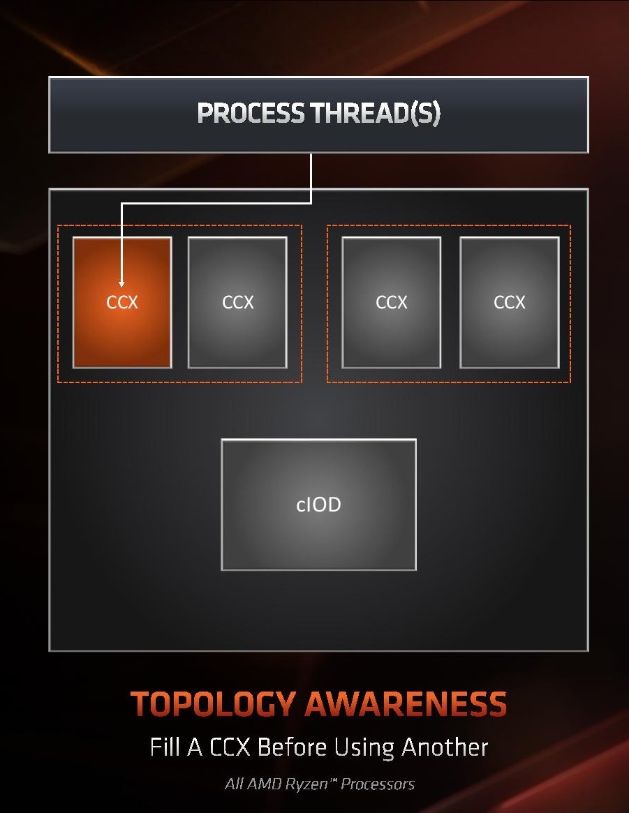
First, what would the benefit of an L4$ be, when the L3$ is 64MB for 12C and 16C, which is massive already (Intel's top chips have 2MB/core - Zen 2 is 4-6MB/core)? Do we know that additional cache beyond the 70+MB total for these higher end chips (or even more than 32MB for the 8C/16T) would help? I know larger L3$ on Intel chips did provide a performance boost, mild, but is there a tipping point for performance, or a limit beyond which L3$ size loses benefit? I only ask because I hear L3$ is expensive, not just cash wise, but also for space.
Second, assuming an additional cache layer with L4$ would be beneficial, why wouldn't it be implemented into the I/O chiplet, and make the I/O chiplet just a little bigger? It seems there is plenty of space for expansion of the I/O.
Third, based on the routing layout we saw, it looks like the power delivery system is already a sizeable portion of the chip, meaning it seems with this layout, 16 cores seems to be the limit. If the power delivery areas were increased 50% to accommodate another chiplet to do 24 cores, it seems there wouldn't be enough room to squeeze the extra chiplet in.
Finally, and I'm sure this has a good reason, if you look at the length of the IF connects between chiplet and I/O, wouldn't it make sense to stretch the I/O die horizontally and make the IF links straight, move the I/O chiplet closer to the CCX (
see here for routing map) so that the IF links would be as short as possible between chiplet and I/O? And if it's true that the dark purple at the right of the I/O is for peripherals, wouldn't it make sense to move that to the south side of the I/O chiplet and move the DDR4 memory links to the right side? Again, not a CPU engineer, but in my rudimentary mind, shorter lines may save a nanosecond here or there.


.png")
.png")
.png")

.png")
.png")
.png")