Speculation: Ryzen 4000 series/Zen 3

Page 71 - Seeking answers? Join the AnandTech community: where nearly half-a-million members share solutions and discuss the latest tech.

uzzi38

Platinum Member
Oct 16, 2019
2,607
5,822
146
Man, I don't know why you are going off on a tangent, especially when you ended up agreeing with my original comment(which you tried to counter). Your response was specifically to my comment:

I responded to your follow up comment and the performance figures you claimed there AFTER stating you made the right choice by looking at the overclocked bench. I conceded on that point already.

Obviously we can all see that userbenchmark's "8 cores" isn't really 8 physical cores otherwise the max, "64 cores" won't improve. There's no way to distinguish between cores and threads when the program supports anything between 1 and Max. For simplicity's sake we take note of ST results, and MT.

Uh, yes you can. There is a way to distinguish - physical cores get loaded first, then logical ones afterwards. Have you ever actually run the benchmark yourself? It always does the same thing ever time. Physical cores first, logical ones second. So in the context of ICL-U and Renoir:

UB : ICL-U - RNR
1 core: 1 core - 1 cores
2 cores: 2 cores - 2 cores
3 cores: 3 cores - 3 cores
4 cores: 4 cores - 4 cores
5 cores: 4 cores 1 thread - 5 cores
6 cores: 4 cores 2 threads - 6 cores

And you get the idea. This is fully repeatable, every time you do the benchmark.

There are laptops beyond the Spectre and XPS you know? You just didn't look hard enough.

The HP Pavillions, Inspirons, and the unnamed Lenovos you can find with Icelake. Many don't use LPDDR4x memory. Heck, many don't even include a second memory channel! Yes and they are DDR4-2666. And I can find them in userbenchmark too. Just look at bandwidth figures. And they will impact CPU performance.

Fair enough. But I mean, I already conceded on this point, so w/e.
 

eek2121

Platinum Member
Aug 2, 2005
2,929
4,000
136
On a realistic note, I expect AMD to focus on clock speeds for Zen 3 primarily, though I also expect a 10-15% IPC improvement (the revealed architectural changes alone would have us at least halfway there). Clock speed is actually a pretty low hanging fruit for Zen 3. Zen 2 was limited partially by using the chiplet design because it had a separate IO die eating up nearly a third of the power budget (from what I've been able to gather from various users, I do not have a zen 2 chip). Zen 2 will also utilize 7nm EUV (unless AMD flips the tables) which has a reported (per TSMC) 10% efficiency improvement. Many Zen 4 chips are hitting 4.3-4.5 GHz, and I've seen at least 1 user get 1 CCX of a 3950X to 4.875 GHz with the remaining cores locked in at 4.5 GHz.

Given this, I expect that any clock speed advantage that Intel has currently will likely disappear, and what few benchmark wins they have left along with it.

btw, for those that are curious, source on the 4.875/4.5 GHz overclock: https://www.chiphell.com/forum.php?mod=viewthread&tid=2169723&extra=page=1&filter=typeid&typeid=220
 

IntelUser2000

Elite Member
Oct 14, 2003
8,686
3,785
136
Zen 2 will also utilize 7nm EUV (unless AMD flips the tables) which has a reported (per TSMC) 10% efficiency improvement. Many Zen 4 chips are hitting 4.3-4.5 GHz, and I've seen at least 1 user get 1 CCX of a 3950X to 4.875 GHz with the remaining cores locked in at 4.5 GHz.

At some point in the 4GHz mark(4.1, 4.2, 4.3...), its not limited by transistors as much as thermals. Coffeelake gets to 5GHz because its using >150W.

5GHz isn't new, but in the Pentium 4 days even the top heatsinks were much, much smaller, and watercooling was almost in the exotic cooling range. As long as you had the proper cooling, you could get there.

When it comes to peak clocks, you can basically disregard Intel's claims with the + on their 14nm process. Skylake could do 4.6GHz, Kabylake 4.8GHz, Coffeelake 4.9GHz, and the refresh of that 5GHz. Cometlake is 5.1GHz, but some lucky cores may reach 5.2 only in single thread, and that particularly lucky core might do 5.3GHz for 10 milliseconds. If you want 5.2/5.3GHz to be the constant, under load clock, then you have to use water cooling. Nothing has changed in the 15 years.

Sure the base clocks have went up a lot but that just means they got that much better at sorting the chips or whatever.

I expect both AMD and Intel clocks to go down, unless they want to start pushing WC setups as the new normal. Do you want them to focus on performance or clocks?

Uh, yes you can. There is a way to distinguish - physical cores get loaded first, then logical ones afterwards. Have you ever actually run the benchmark yourself? It always does the same thing ever time. Physical cores first, logical ones second. So in the context of ICL-U and Renoir:

Ok fair points. I still don't put stock in inbetween results as Windows benchmarking is that finicky. If you want to look at it in general, sure why not. If you want to see perf/clock differences that might separate the chips by few %, no way.
 
  • Like
Reactions: Tlh97

insertcarehere

Senior member
Jan 17, 2013
639
607
136
On a realistic note, I expect AMD to focus on clock speeds for Zen 3 primarily, though I also expect a 10-15% IPC improvement (the revealed architectural changes alone would have us at least halfway there). Clock speed is actually a pretty low hanging fruit for Zen 3. Zen 2 was limited partially by using the chiplet design because it had a separate IO die eating up nearly a third of the power budget.

So is Zen 3 going to abandon chiplets and go monolithic even for HEDT/EPYC? I find it hard to believe that AMD would pull such a u-turn given Zen/Zen 2 were all designed with chiplets/MCM in mind.
 

eek2121

Platinum Member
Aug 2, 2005
2,929
4,000
136
So is Zen 3 going to abandon chiplets and go monolithic even for HEDT/EPYC? I find it hard to believe that AMD would pull such a u-turn given Zen/Zen 2 were all designed with chiplets/MCM in mind.

Renoir is using a monolithic design. I personally wouldn't rule the chiplet design out, however if all components are on 7nm EUV then one could argue there is little reason to break them out.
 

IntelUser2000

Elite Member
Oct 14, 2003
8,686
3,785
136
Renoir is using a monolithic design. I personally wouldn't rule the chiplet design out, however if all components are on 7nm EUV then one could argue there is little reason to break them out.

The reason chiplets make sense for high end workstation/gaming laptops and desktops/servers is because power consumption matters much less and going to a new process is becoming more difficult and more expensive.

Sure, over time the cost comes down, but its the upfront cost that's increasing.

Plus, I/O components do not benefit from new process as digital logic and cache does. This is why the integrated thunderbolt controller is so large on Icelake. I/O isn't so stringent on performance requirements either.

Therefore, its beneficial to leave I/O a process generation or more behind and reap the benefits of not only cheaper costs, but in some cases lower leakage current.

Costs also rise nonlinearly with die size and yields drop too. Chiplets combat that by specializing the dies more and more to their usage cases.
 
  • Love
Reactions: spursindonesia

uzzi38

Platinum Member
Oct 16, 2019
2,607
5,822
146
On a realistic note, I expect AMD to focus on clock speeds for Zen 3 primarily, though I also expect a 10-15% IPC improvement (the revealed architectural changes alone would have us at least halfway there). Clock speed is actually a pretty low hanging fruit for Zen 3. Zen 2 was limited partially by using the chiplet design because it had a separate IO die eating up nearly a third of the power budget (from what I've been able to gather from various users, I do not have a zen 2 chip). Zen 2 will also utilize 7nm EUV (unless AMD flips the tables) which has a reported (per TSMC) 10% efficiency improvement. Many Zen 4 chips are hitting 4.3-4.5 GHz, and I've seen at least 1 user get 1 CCX of a 3950X to 4.875 GHz with the remaining cores locked in at 4.5 GHz.

Given this, I expect that any clock speed advantage that Intel has currently will likely disappear, and what few benchmark wins they have left along with it.

btw, for those that are curious, source on the 4.875/4.5 GHz overclock: https://www.chiphell.com/forum.php?mod=viewthread&tid=2169723&extra=page=1&filter=typeid&typeid=220

Zen 3 will hardly bump clocks for desktop. If at all.

Also, chiplet is here to stay for the time being. You're not entirely correct on the power draw part, the chiplet solution itself only adds 12-18W of power (1-2 chiplets), primarily through the I/O die itself pulling quite a bit of power. But if you include in the idle power draw coming from the rest of the uncore, that can hike up to about 30W. Take for example, a PPT (power pulled from the socket) of 45W, the CPU cores will be given a mere 15W to distribute between them. See this: https://cdn.discordapp.com/attachme.../Screenshot_20191230-225505_Samsung_Notes.jpg

These are taken from R20 runs. Were this a monolithic solution, the cores would only be getting an extra 12W of power than they are here. The rest of the power draw is from the I/O itself - and this would remain whether or not it's in the same or a separate die.
 

DisEnchantment

Golden Member
Mar 3, 2017
1,601
5,769
136
Also, many patents for cpu's front end latency, decode, uop and L1 cache latency
Indeed.

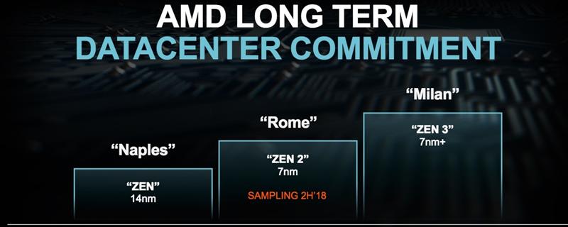
In one of those slides from the leaked event that sparked a long discussion on SMT2 here, I remember the cache were still inside the compute chiplet for Milan. Do you think this patent would apply to a "L4 cache" if used for Milan?

I reread the patent and cross referenced several other patents and it seems the cache control logic is in the Compute block. Not sure about L3.
In most of these patents, it seems to me the cache control is used together with the cache directory for unifying the L3s across the CCDs. And also used in other patents to locate data in cache memory(after L2 i.e. L3/L4?) /data localization.

I think it will not make it to Milan. But the Cache directory will because in the initial patents it is the one 'unifying' the L3.
But we will know more in few hours if we are lucky.
 

eek2121

Platinum Member
Aug 2, 2005
2,929
4,000
136
At some point in the 4GHz mark(4.1, 4.2, 4.3...), its not limited by transistors as much as thermals. Coffeelake gets to 5GHz because its using >150W.

5GHz isn't new, but in the Pentium 4 days even the top heatsinks were much, much smaller, and watercooling was almost in the exotic cooling range. As long as you had the proper cooling, you could get there.

When it comes to peak clocks, you can basically disregard Intel's claims with the + on their 14nm process. Skylake could do 4.6GHz, Kabylake 4.8GHz, Coffeelake 4.9GHz, and the refresh of that 5GHz. Cometlake is 5.1GHz, but some lucky cores may reach 5.2 only in single thread, and that particularly lucky core might do 5.3GHz for 10 milliseconds. If you want 5.2/5.3GHz to be the constant, under load clock, then you have to use water cooling. Nothing has changed in the 15 years.

Sure the base clocks have went up a lot but that just means they got that much better at sorting the chips or whatever.

I expect both AMD and Intel clocks to go down, unless they want to start pushing WC setups as the new normal. Do you want them to focus on performance or clocks?
Intel chips on 14nm can maintain 4.7-4.8 GHz on 6 cores when constrained to a 95 watt TDP. Anandtech has an article on this.

The reason chiplets make sense for high end workstation/gaming laptops and desktops/servers is because power consumption matters much less and going to a new process is becoming more difficult and more expensive.

Sure, over time the cost comes down, but its the upfront cost that's increasing.

Plus, I/O components do not benefit from new process as digital logic and cache does. This is why the integrated thunderbolt controller is so large on Icelake. I/O isn't so stringent on performance requirements either.

Therefore, its beneficial to leave I/O a process generation or more behind and reap the benefits of not only cheaper costs, but in some cases lower leakage current.

Costs also rise nonlinearly with die size and yields drop too. Chiplets combat that by specializing the dies more and more to their usage cases.
Except there won't be yield issues under 7nm EUV. The power gains are from moving from 14nm to 7nm for the IO die, btw.

I am not declaring that they definitely won't use chiplets, only that chiplets can increase packaging costs as well as latency and make the chip harder to cool.

Source?
 

Gideon

Golden Member
Nov 27, 2007
1,619
3,643
136
They will absolutely still use chiplets, at the very least for everything above 8 cores, as they need them anyway for Server and HEDT designs (and that means they need a AM4 IO die anyway)

They will also almost assuredly use them for 6-8 core desktop chips as well, as they will not release a new APU so close to Renoir (it will come Q1 2021) and making an expensive monolithic desktop die that they can only sell in the rather small desktop market.
 

uzzi38

Platinum Member
Oct 16, 2019
2,607
5,822
146
Bit of logic they won't be shifting to monolithic for desktop Zen 3. No point in diversifying Desktop/Server so much just yet - it's a big cost investment for little gain. We know for a fact server is still chiplets, see the leaked AMD slides about unified L3 - those slides also showed Milan being chiplet based iirc.

Though, even if they didn't, they did also show a chiplet having it's L3 merged, so both work I guess.

Anywho, if server is still chiplet, desktop is still chiplet. There's no real benefits to switching desktop to monolithic yet, heck, there might never be. Desktop isn't too bothered by power consumption, and it works as a great cost cutting measure by having the poorly scaling I/O on 12nm (and maybe 12nm+ later). Chiplet might even improve thermals mind you - just by spacing out the parts of the CPU with the greatest thermal density.

Renoir is monolithic because it would be nonviable as a mobile product if it wasn't, and because it's so small it doesn't matter anyway. A rough guess puts it around or below 140mm^2 (assuming 8 cores, 8 CUs and 4MB L3 per CCX). It's not proof of AMD switching back to monolithic or anything like that.
 

maddie

Diamond Member
Jul 18, 2010
4,738
4,667
136
Intel chips on 14nm can maintain 4.7-4.8 GHz on 6 cores when constrained to a 95 watt TDP. Anandtech has an article on this.


Except there won't be yield issues under 7nm EUV. The power gains are from moving from 14nm to 7nm for the IO die, btw.

I am not declaring that they definitely won't use chiplets, only that chiplets can increase packaging costs as well as latency and make the chip harder to cool.


Source?
Total costs mister. Chiplets are a lot cheaper overall for this scenario. By AMD's own estimates for Zen1, they were 59% the cost of a monolithic equivalent.

aHR0cHM6Ly9pbWcucHVyY2guY29tL3cvNTAwL2FIUjBjRG92TDIxbFpHbGhMbUpsYzNSdlptMXBZM0p2TG1OdmJTODJMelF2TnpBMU1qUTBMMjl5YVdkcGJtRnNMekF5TGxCT1J3PT0=
 

DrMrLordX

Lifer
Apr 27, 2000
21,609
10,803
136

The leaked presentation from 2019 showed the new CCX design and everything. You know, the one they had to pull from Youtube? It's common knowledge by now.

edit:


That came out months ago.
 
Last edited:

moinmoin

Diamond Member
Jun 1, 2017
4,944
7,656
136
While Renoir will still be based in Zen 2, like the previous APUs it will contain microcode of the next Zen gen, so Zen 3 in this case. If the rumor of Renoir having 8 cores is correct (and it prolly should be, with Intel increasing the number of cores as well), this would mean two CCXs with 4 cores each. The "next gen" microcode would have to handle the increasing latency two CCXs would otherwise introduce while retaining the significantly smaller L3$ size of APUs compared to the server/desktop dies.

To me it sounds like DisEnchantment's interpretation of the patents is spot on (assuming compute block = CCX, so definitely L3$):
I reread the patent and cross referenced several other patents and it seems the cache control logic is in the Compute block. Not sure about L3.
In most of these patents, it seems to me the cache control is used together with the cache directory for unifying the L3s across the CCDs. And also used in other patents to locate data in cache memory(after L2 i.e. L3/L4?) /data localization.
 

liahos1

Senior member
Aug 28, 2013
573
45
91

Is videocardz.com legit? Seems like respectable parts
 

Attachments

  • Ryzen 4000.png
    Ryzen 4000.png
    41.3 KB · Views: 28

DiogoDX

Senior member
Oct 11, 2012
746
277
136

Is videocardz.com legit? Seems like respectable parts
they are just showing those:


amd6502

Senior member
Apr 21, 2017
971
360
136
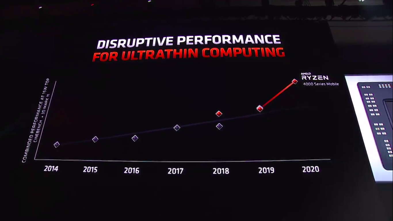
For an 8c/16t that's ultra low power. Very nice. Any higher gpu power laptop will simply come with dGPU and have the iGPU just for long battery life ability.

8CU at peak perf watt freq will provide nice > 720p-hi settings ability.

For desktop SKUs they can run hot near peak perf freq, and the 8CU will match 12nm Vega 11 CU (and bandwidth would limit perf anyways unless using very pricey high freq DDR4).
 
  • Like
Reactions: spursindonesia