Speculation: Ryzen 4000 series/Zen 3

Page 29 - Seeking answers? Join the AnandTech community: where nearly half-a-million members share solutions and discuss the latest tech.

Tuna-Fish

Golden Member
Mar 4, 2011
1,346
1,525
136
I am confused. As I understand it, cores are, as you say, directly attached to their L3 slice. However, the 4 slices in the current CCX are fully connected with 6 bidirectional links. I haven't seen this number 16 claimed anywhere else. Can you draw a diagram to explain what you mean? See my topology discussion for reference.

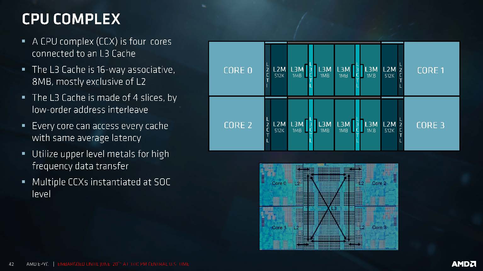
There are no links between "slices of CCX". There are two things in the system, cores and cache slices. Each core is directly connected to each of the 4 cache slices with a dedicated link. One of the cache slices is physically closest to the core, but this does not in any way make it "its" slice. All physical addresses are hashed over the 4 slices based on lowest-order bits of their cache set address. So every core accesses each L3 slice equally. Communication between the L2 of one core and the L2 of another is done through the relevant L3 slice, which holds some additional tags for lines not currently in L3 but in the L2 of some core.

So there are 16 dedicated bidirectional links between the cache slices and the cores.

To reiterate: L3 slices are only attached to cores, and cores are only attached to L3 slices. In a diagram, there should be no lines from L3 to another L3, or from core to another core. As an image:
vJyEIYZ.png

The thing I have marked in green is NOT any kind of logical or physical unit. I can see why some would think that it is, because with Intel there is such an unit, but for AMD there isn't. The connection between the L2CTL of Core 1 has exactly the same kind of connection to the L3CTL cache slice I have marked "B" as it has to cache slices A, C and D.
 
Last edited:

Vattila

Senior member
Oct 22, 2004
799
1,351
136
So there are 16 dedicated bidirectional links between the cache slices and the cores.

I understand what you mean now: You claim each core directly accesses all of the four slices with a dedicated link, thus 4 x 4 = 16 links. That seems wasteful, though, and I have not seen it claimed elsewhere. Do you have a reference?

My understanding, from all the material and discussions I have seen, is that the core makes a request to its L3 slice, and the request is then redirected to one of the other three slices as needed based on the address. This requires 6 links to avoid extra hops.

(You can see these 6 links between slices drawn in AMD's slides.)

amd-ccx-epyc-cpu-presentation-slides-1.jpg


As you say, the L3 cache is using an interleaved memory scheme. As I understand it, this is done to achieve uniform access latency on average, since access latency differs for local slice and remote slice (1 hop away). If all cores had a direct link to each slice, as you claim, there would not be a need to do any interleaving, as the access latency would be fully uniform whatever slice accessed. Actually, I would see no need to slice up the L3 at all if this was the case. Why not just have a monolithic L3 cache with 4 access ports?

So although I am a complete novice in this, I am not convinced you have the correct understanding of the implementation. Please clarify and provide links if you can.
 
Last edited:
  • Like
Reactions: extide and Kirito

Tuna-Fish

Golden Member
Mar 4, 2011
1,346
1,525
136
I understand what you mean now: You claim each core directly accesses all of the four slices with a dedicated link, thus 4 x 4 = 16 links. That seems wasteful, though, and I have not seen it claimed elsewhere. Do you have a reference?

My understanding, from all the material and discussions I have seen, is that the core makes a request to its L3 slice, and the request is then redirected to one of the other three slices as needed based on the address. This requires 6 links to avoid extra hops.
This is very clearly disproven in the slide I linked above, and also by practical testing. Every core has equal latency access to each 4 slices. There are no additional hops.

As you say, the L3 cache is using an interleaved memory scheme. As I understand it, this is done to achieve uniform access latency on average, since access latency differs for local slice and remote slice (1 hop away). If all cores had a direct link to each slice, as you claim, there would not be a need to do any interleaving, as the access latency would be fully uniform whatever slice accessed. Actually, I would see no need to slice up the L3 at all if this was the case. Why not just have a monolithic L3 cache with 4 access ports?

So although I am a complete novice in this, I am not convinced you have the correct understanding of the implementation. Please clarify and provide links if you can.

Making a single cache controller that can handle 4 requests per clock is much harder than making a cache controller that can handle a request per clock, and then duplicating it 4 times. Interleaving the addresses means that every core uses every slice equally, distributing the workload among the 4 L3 slices.
 

Vattila

Senior member
Oct 22, 2004
799
1,351
136
This is very clearly disproven in the slide I linked above, and also by practical testing. Every core has equal latency access to each 4 slices. There are no additional hops.

It is far from clear to me. Note that your slide says "same average latency". This is achieved by the memory address interleaving between cache slices. Perhaps this is what has thrown off your understanding? Or do you have other references on which you base your understanding?

PS. I've added an AMD slide in my previous post, that clearly indicate that there are 6 links. This slide also says "same average latency".
 
Last edited:
  • Like
Reactions: extide

Ajay

Lifer
Jan 8, 2001
15,430
7,849
136
The thing I have marked in green is NOT any kind of logical or physical unit. I can see why some would think that it is, because with Intel there is such an unit, but for AMD there isn't. The connection between the L2CTL of Core 1 has exactly the same kind of connection to the L3CTL cache slice I have marked "B" as it has to cache slices A, C and D.

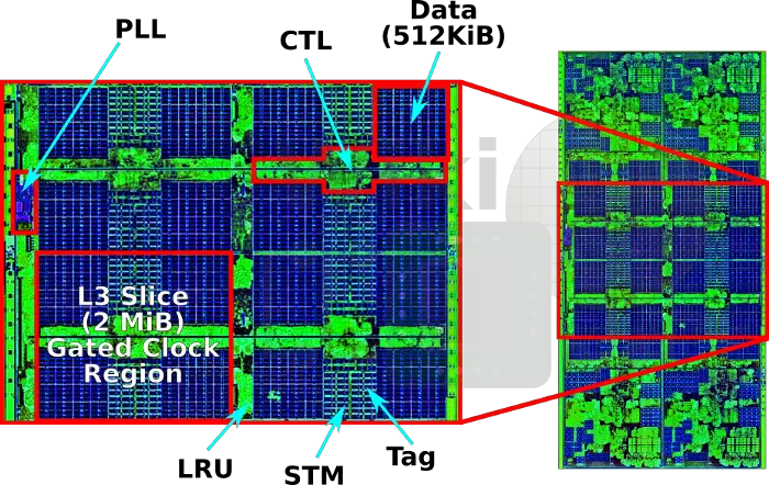
there is some physical reality to the actual die layout as shown from this image from Wikichip:
2018-amd-conf-ccx-l3.png

The core L2$s are along the top and bottom edges of the red box and the very top and bottom are the CPU’s core logic (well, and uncore, as this is Zen1).


It is far from clear to me. Note that your slide says "same average latency". This is achieved by the memory address interleaving between cache slices. Perhaps this is what has thrown off your understanding? Or do you have other references on which you base your understanding?

PS. I've added an AMD slide in my previous post, that clearly indicate that there are 6 links. This slide also says "same average latency".

I believe that AMD uses the term ‘average latency' because the are small differences in latency due to routing times (path length). So, technically, the latency isn’t identical - but from a low level programming standpoint, however, they are the same. IMO.
 
  • Like
Reactions: Vattila

Vattila

Senior member
Oct 22, 2004
799
1,351
136
I believe that AMD uses the term ‘average latency' because the are small differences in latency due to routing times (path length).

Exactly. My understanding is that an access to a remote slice requires a hop across the slice interconnect (6 links) as indicated on AMD's slides (see my previous post #703). Effective latency is averaged out by memory address interleaving.

Is it your understanding that there are 16 links, as claimed by Tuna-Fish? If so, why?
 
Last edited:

Ajay

Lifer
Jan 8, 2001
15,430
7,849
136
Making a single cache controller that can handle 4 requests per clock is much harder than making a cache controller that can handle a request per clock, and then duplicating it 4 times. Interleaving the addresses means that every core uses every slice equally, distributing the workload among the 4 L3 slices.

Yeah, this is what i don’t get about Zen 3s 'unified' L3 cache. How on earth do 8 cores access one access 32MB (or more) cache block? Obviously, AMD has people much smarted than I working on this - it is a puzzle.

Exactly. My understanding is that an access to a remote slice requires a hop across the slice interconnect (6 links) as indicated on AMD's slides (see my previous post #703). Effective latency is averaged out by memory address interleaving.

Do you have an understanding that there are 16 links, as claimed by Tuna-Fish? If so, why?

What Tuna-Fish said made sense, but then there is that pesky 6 link slide from AMD. Six links are doable, and don’t require an extra hop. In the enhanced die shot in my above post, you can see two thick green horizontal bars with the 4 L3CTL units on them and then the thick green vertical line down the center - those thick green bars are mainly wires. The diagonal L3s don’t need a hop, they just need a longer wire from one L3CTL to another. Hence the small difference in latency (propagation delay). I haven’t found any authoritative commentary on Zen1 or Zen2’s cache architecture - despite my web search efforts; you’d think there would be a Hotchips video out there.
 
  • Like
Reactions: Vattila

Vattila

Senior member
Oct 22, 2004
799
1,351
136
What Tuna-Fish said made sense,

Why do 16 links make sense over 6? To my limited understanding, 16 links are a lot, if not prohibitive. So why presume 16 when AMD's slides clearly indicate 6? Why 16, when network topology theory says that 6 links are what you need to fully connect 4 nodes? What is the technical argument? Where is the evidence in form of references?

you’d think there would be a Hotchips video out there.

AMD Fellow and Lead Architect of Zen, Mike Clark, had a presentation on the Zen architecture back at HotChips 2016 (here). Unfortunately, he does not go into sufficient detail to fully clarify this point beyond any doubt. But all that he says and shows on his slides is fully compatible with my understanding that there are 6 links between the L3 slices.

I think he gets this [belief in 16 links] from the slide you posted before, it says 16 way on the second bullet point: [The L3 cache is 16-way associative...]

:)

Are you mocking us now? Cache associativity has nothing to do with topology, of course.
 
Last edited:
  • Like
Reactions: Kirito

soresu

Platinum Member
Dec 19, 2014
2,657
1,858
136
I must be mad then, because I count 20 total L3 links on that cache diagram.

2 for each core to an L3 slice (x8), and 2 between each slice of the L3 (x12).
 

Vattila

Senior member
Oct 22, 2004
799
1,351
136
I must be mad then, because I count 20 total L3 links on that cache diagram.

Divide by two. We are talking about bidirectional links. Then subtract four for the L2 to L3 links internal to each core (I am not counting those). That gives you 6 — which is the number of links you need to fully connect the 4 cache slices.
 
Last edited:

Vattila

Senior member
Oct 22, 2004
799
1,351
136
this is what i don’t get about Zen 3s 'unified' L3 cache. How on earth do 8 cores access one 32MB (or more) cache block?

To interconnect 8 cache slices, AMD can use the cube topology I proposed (post #699). This requires an extra port on each slice, and four links between them, for a total of 6 + 6 + 4 = 16 links. This topology has a network diameter of only 2 hops. To average out latency they can continue to use memory interleaving, just by using another bit in the address to discriminate the destination slice.

PS. As I wrote in post #666, this topology is a simple evolution of the current 4-core CCX that may offer configurability: "If they use the 2x4 topology I propose (in the CCX thread), they may be able to offer two BIOS configurations for the chiplet, i.e. two separate 4-core CCXs (NUMA), each with a private 32 MB of low-latency L3 cache (1 hop diameter), or an 8-core CCX (UMA), with 64 MB of higher-latency L3 cache (2 hops diameter)."
 
Last edited:

NostaSeronx

Diamond Member
Sep 18, 2011
3,686
1,221
136
I never expected SMT4, I'm just glad that dumb meme has been shot down :)
It technically hasn't been shot down... there is still Zen2 consoles(Family 17h greater than 30h) and Zen3 Ryzen(Family 19h Models 20h-2Fh).

The info dropped:
Milan is still using octo-core chiplets, it has 8 CCD compatibility with Rome. It still has 64-cores and 2x thread per core, in the 9-die config.

It looks like Oracle's M7/M8 cache architect is doing Zen3's L3 cache. For M7 comparison => https://www.nextplatform.com/2015/10/28/inside-oracles-new-sparc-m7-systems/
Potentially, a return to point-2-point with a server-orientated L3 version of Jaguar's L2.
 
Last edited:
  • Like
Reactions: Kirito and amd6502

Ajay

Lifer
Jan 8, 2001
15,430
7,849
136
Why do 16 links make sense over 6? To my limited understanding, 16 links are a lot, if not prohibitive. So why presume 16 when AMD's slides clearly indicate 6? Why 16, when network topology theory says that 6 links are what you need to fully connect 4 nodes? What is the technical argument? Where is the evidence in form of references?

So, basically I agreed with you (rather, the AMD slide). There are 6 links (fully connected mesh), they are each bidirectional (R/W). Each core's L2$ Is connected 1:1 with it's closest L3 slice. I cant find the byte width of L2 to L3, L1 to L2 is 32 bytes. I’m going to assume it is also 32B (to support AVX2 datawidth throughout The cache structure). I’ll also assume L3 to L3 of 16B, which would match the 16B width from L3 to memory (via IF). So for each L3 cache controller there are 5 bidirectional ports. 32 bytes from L2, 3 x 16 bytes to connect to nodes L3 cache controller and 16 bytes out to memory. These are bidirectional, so each of these links are actually 2x the width. So the number of wires coming in and out of L3CTL = 2*(32 + 3*16 + 16)*8 = 1536!!! Just the L3 mesh is 768 wires (for each bit, obviously) from one node to the other three!

So, what is the point of all this? To be clear that whatever path AMD has chosen for Zen3's 8 core CCX, they were very mindful the amount of wiring that is required to do so. Die usage shouldn’t be an issue, since I think they can use a higher metal layer for that - but power usage vs performance was certainly a design choice they had to make.
No surprises as to why Intel choose a ring.
 

Ajay

Lifer
Jan 8, 2001
15,430
7,849
136
To interconnect 8 cache slices, AMD can use the cube topology I proposed (post #699). This requires an extra port on each slice, and four links between them, for a total of 6 + 6 + 4 = 16 links. This topology has a network diameter of only 2 hops. To average out latency they can continue to use memory interleaving, just by using another bit in the address to discriminate the destination slice.
What slices? The presentation summary said a unified cache. I’ve seen dual ported caches before, but Octo-ported, WTH?

edit - got auto corrected.
 
Last edited:
  • Like
Reactions: Vattila

jamescox

Senior member
Nov 11, 2009
637
1,103
136
Technically PCIe4-ESM is 25GT/s so they're even.

Yes, also what's the use for BIGGUR SMT if you're not IBM trying to game per-C licensing?

That doesn’t seem to be a part of the pci-express 4.0 standard, which is 16 GT/s.
 
Mar 11, 2004
23,073
5,554
146
With regards to the SMT4 talk. I think that was largely academic in its discussion (i.e. "if they were going to do that, here's things that support that as a possibility") and just generally discussing if doing that makes sense versus increasing core counts. I don't entirely get the derision that some people have with regards to obvious speculation (although I've probably done the same about other things that I thought it was silly for people to speculate about; Nosta's nonsense comes to mind).

I don't think there was any indication that was being worked on, but rather people took something known (well established via industry rumor), and speculating about what that was (with I think people just assuming it was SMT4 as that's been established and would possibly make some sense with other things AMD has done).

Which, I believe this was all borne out of the rumor that there were Xbox dev kits that had Zen CPUs that could do more than 2 threads per core. If I remember correctly it was only like 3 threads, and the stuff I read that was being talked about sounded quite different from normal SMT stuff (I remarked at the time that it reminded me of the rumored "reverse hyperthreading" that used to be talked about). Now, perhaps AMD has been working on some new SMT stuff, or perhaps it was some specialization done for Microsoft's testing, and maybe its something that would only be feasible in a pretty locked down environment (say a gaming console) or if you disregard security (so maybe you'd use it to boost throughput for say video encoding or say doing video game processing) and is more about the software than the hardware (meaning it wasn't AMD but rather Microsoft behind it and they were seeing if properly coded they could push 3 threads through instead of just 2), and that the Xbox dev kits just provided a really good platform for testing it out. Heck, maybe it was testing being done with regards to the speculative execution stuff.

I'm not terribly shocked to find AMD isn't upping core or thread counts on Zen 3. There's not much gains in the process, and seems like they don't need to push it quite as hard, plus if they keep iterating like they have been, they can bring those boosts at 5nm. Also, frankly, seems like there's room for quite a bit of maturing in the platform. Which if the transition of Zen 2 to 3 is equal to Zen to Zen+ I think that'll be pretty good, and anything more will be extra nice.

So, how exactly would the HBM connect to the IO die it is stacked on without having TSVs in the IO die, making it equivalent to an active interposer?p For low performance stuff (like mobile or NAND flash die), they sometimes do stacking by just offsetting the chips and using essentially little wires attached to the edge of the chips (similar to old style wire bonding). That might be fine for a DDR channel or NAND interface, but not for a 1024-bit HBM bus.

It was my understanding that the TSVs are there in order to connect higher stacks directly through the lower ones (so if you weren't trying to connect higher stacks, you wouldn't have the TSVs).

I would assume you'd use microbumps just like they were using to connect the HBM to the interposer. AMD has already talked about how they've had to resort to some new stuff to connect Zen 2 chips to the packaging substrate, and they've said they've been checking out stacking and similar.

I would also assume they'd rework the I/O die to facilitate a stacking interface. But since the I/O die is directing everything, its not like the HBM would need a direct to package interface.

Plus, like I said, maybe they could fab HBM right into the I/O die itself when its just simply cache. That'd take care of stacking. Then in the future they could just design the packaging so it basically has an interposer layer for HBM stacks.
 

jamescox

Senior member
Nov 11, 2009
637
1,103
136
With regards to the SMT4 talk. I think that was largely academic in its discussion (i.e. "if they were going to do that, here's things that support that as a possibility") and just generally discussing if doing that makes sense versus increasing core counts. I don't entirely get the derision that some people have with regards to obvious speculation (although I've probably done the same about other things that I thought it was silly for people to speculate about; Nosta's nonsense comes to mind).

I don't think there was any indication that was being worked on, but rather people took something known (well established via industry rumor), and speculating about what that was (with I think people just assuming it was SMT4 as that's been established and would possibly make some sense with other things AMD has done).

Which, I believe this was all borne out of the rumor that there were Xbox dev kits that had Zen CPUs that could do more than 2 threads per core. If I remember correctly it was only like 3 threads, and the stuff I read that was being talked about sounded quite different from normal SMT stuff (I remarked at the time that it reminded me of the rumored "reverse hyperthreading" that used to be talked about). Now, perhaps AMD has been working on some new SMT stuff, or perhaps it was some specialization done for Microsoft's testing, and maybe its something that would only be feasible in a pretty locked down environment (say a gaming console) or if you disregard security (so maybe you'd use it to boost throughput for say video encoding or say doing video game processing) and is more about the software than the hardware (meaning it wasn't AMD but rather Microsoft behind it and they were seeing if properly coded they could push 3 threads through instead of just 2), and that the Xbox dev kits just provided a really good platform for testing it out. Heck, maybe it was testing being done with regards to the speculative execution stuff.

I'm not terribly shocked to find AMD isn't upping core or thread counts on Zen 3. There's not much gains in the process, and seems like they don't need to push it quite as hard, plus if they keep iterating like they have been, they can bring those boosts at 5nm. Also, frankly, seems like there's room for quite a bit of maturing in the platform. Which if the transition of Zen 2 to 3 is equal to Zen to Zen+ I think that'll be pretty good, and anything more will be extra nice.


It was my understanding that the TSVs are there in order to connect higher stacks directly through the lower ones (so if you weren't trying to connect higher stacks, you wouldn't have the TSVs).

I would assume you'd use microbumps just like they were using to connect the HBM to the interposer. AMD has already talked about how they've had to resort to some new stuff to connect Zen 2 chips to the packaging substrate, and they've said they've been checking out stacking and similar.

I would also assume they'd rework the I/O die to facilitate a stacking interface. But since the I/O die is directing everything, its not like the HBM would need a direct to package interface.

Plus, like I said, maybe they could fab HBM right into the I/O die itself when its just simply cache. That'd take care of stacking. Then in the future they could just design the packaging so it basically has an interposer layer for HBM stacks.

There are TSVs in the HBM stacks, but the interposer also has TSVs.

Most modern, high performance chips are flip chips. They take the wafer and make a bottom layer of transistors. Then many layers of interconnect are sandwiched between insulating layers. The interconnect generally gets larger the higher it is up in the stack. Basically, they will have some set of low level cells that defines some small amount of transistors with connections in maybe layers 1 and 2. Then many types of such low level cells are placed and interconnected in the next layers up, maybe layers 3 and 4. That continues with the top metal layers being connections between large functional units. The top layer will actually be where the solder bumps are placed for routing off die. The wafer is diced up then solder bumps or micro bumps are placed on top. The chip is flipped over such that the solder bumps are on the bottom. Once it is flipped, the silicon wafer is on top, then the transistor layers, then the interconnect layers. You can’t mount anything on top since the silicon substrate ends up on the top.

To attach something on top, you need TSVs through the interposer. For something like an HBM gpu, I assume that they take a wafer and etch holes for the TSVs and fill them with metal. For an active interposer, they would do a layer of transistors. For either one, they will then do layers of interconnect as they would for a standard flip chip. The bumps for external interfaces would go on top, but probably after the wafer is diced. There are some technologies that apply bumps prior to dicing. An HBM based GPU still needs a massive number of power and ground pins in addition to the external interfaces; pci-express or infinity fabric links for AMD. After the top metal layers of the interposer are complete, they have to flip the whole wafer over and polish what was the underside of the wafer down to expose the TSVs. They end up with very thin wafers. I am not sure how thin the interposer wafers are. I believe I have seen some stories about the stacked memory wafers being polished down to essentially paper thin (floppy). The interposer can have flip chips with micro-solder balls placed on top, such as gpus, or other stacked devices like the HBM. The HBM stacks use very thin layers since the height has to match the gpu height.

If you look up pictures of interposers, like the images in this article:


The interposer has connections that go all of the way through (TSVs) in addition to the HBM stacks having TSVs internal to the stack.

With how large the L3 cache is getting on AMD parts (32+ MB for Milan), I don’t know if L4 is going to be necessary. Milan should help with any applications that really like large monolithic caches. There are a few applications that do better on intel parts with 38.5 MB available to a single core. If Milan starts at 32 MB and has larger variants, then intel will no longer be competitive for those applications.
 
  • Like
Reactions: Vattila

DrMrLordX

Lifer
Apr 27, 2000
21,620
10,829
136
I don't entirely get the derision that some people have with regards to obvious speculation

SMT4, in particular, made very little sense for AMD's product stack. Also watching people push for SMT4 on mobile platforms strikes me as a bit odd.
 

jamescox

Senior member
Nov 11, 2009
637
1,103
136
To interconnect 8 cache slices, AMD can use the cube topology I proposed (post #699). This requires an extra port on each slice, and four links between them, for a total of 6 + 6 + 4 = 16 links. This topology has a network diameter of only 2 hops. To average out latency they can continue to use memory interleaving, just by using another bit in the address to discriminate the destination slice.

PS. As I wrote in post #666, this topology is a simple evolution of the current 4-core CCX that may offer configurability: "If they use the 2x4 topology I propose (in the CCX thread), they may be able to offer two BIOS configurations for the chiplet, i.e. two separate 4-core CCXs (NUMA), each with a private 32 MB of low-latency L3 cache (1 hop diameter), or an 8-core CCX (UMA), with 64 MB of higher-latency L3 cache (2 hops diameter)."

I think the image showing “6 links” is an inaccurate oversimplification. It does not match with the rest of the information. You do not have 4 slices that need to be connected together, you have 8 things that need to be connected together, 4 cores and 4 cache slices. That image gives the idea that cache slices are connected to each other while the rest of the information indicates that they are not.

It is unclear how large of a chunk is interleaved between caches. Byte interleave seems too small. Perhaps a 32 byte cache line is interleaved across the 4 slices. They have shown slides with 32 bytes a cycle. That would be 8 bytes/64-bits from each cache slice. It is also unclear what you think a “link” is. We are talking about on chip here with nanosecond latency. A “link” is literally just a wire. I expect that it is 4 sets of read and write wires going from each core to each cache slice. If they kept the same architecture, then expanding to 8 could mean going up to 8 sets of wires from each core to 8 cache slices. Note that it could be the same number of wires; it could be 4 bytes x 8 rather than 8 bytes x 4 or something like that. I don’t know if they would do that since that would still be 32-bytes a cycle, except spread across 8 cores instead of 4. They may need to increase to 64 bytes a cycle.

Also note that very wide connections are possible on die. HBM is kind of in between, with the routing in a silicon interposer rather than an organic package. It uses 1024-bit bus per stack, so the 4 stack devices actually have a 4096-bit (512-byte) bus on the gpu. The 32 bytes per cycle from L3 doesn’t really seem that large. The problems come from long interconnect wires driven at high clock. This takes a lot of power. The Pentium 4 actually had pipeline stages just to drive signals across the chip since it was originally designed to reach very high clock that it never achieved due to power limitations. You don’t want to send data long distance. This is probably part of why current intel chips are so power hungry. They don’t really have anything to keep data in local caches, so it ends up transferring data long distances at high clock.

I don’t know how AMD’s 32 MB cache is actually implemented. It may be that some other architecture makes more sense rather than just widening or rearranging the current architecture. Cache designs are actually very complicated to achieve such low latency. The interconnect doesn’t really cost die area since it is mostly wires in the upper metal layers. The connections will just be routed on top of the cache slices. The die could look almost exactly the same since it is the same number of cores and the same number of slices, just connected together differently. They may be able to shrink the cache size quite a bit with EUV 7 nm process, which would shorten the interconnect.
 
  • Like
Reactions: Vattila