Speculation: Ryzen 4000 series/Zen 3

Page 30 - Seeking answers? Join the AnandTech community: where nearly half-a-million members share solutions and discuss the latest tech.

itsmydamnation

Platinum Member
Feb 6, 2011
2,731
3,063
136
t is unclear how large of a chunk is interleaved between caches. Byte interleave seems too small. Perhaps a 32 byte cache line is interleaved across the 4 slices. They have shown slides with 32 bytes a cycle. That would be 8 bytes/64-bits from each cache slice. It is also unclear what you think a “link” is.
This is covered in the Q&A i posted, each core can write or read 32 bytes a cycle to the L3 cache (which ever way it hashes). each slice of the L3 has a buffer ( so multiple core can write to the same L3 slice each cycle). it is unclear if each slice can read and write 32 bytes a cycle or just read or write 32 bytes a cycle.
 

jamescox

Senior member
Nov 11, 2009
637
1,103
136
SMT4, in particular, made very little sense for AMD's product stack. Also watching people push for SMT4 on mobile platforms strikes me as a bit odd.
It could make quite a bit of sense for actual server applications. It makes little sense for just about any other application though. A lot of people seem to lump HPC and other specialized applications, like render farms, in with general servers when they have quite different requirements.

It may not be that difficult to implement once they have a working SMT2 implementation. I didn’t write it off as impossible or preposterous, it is just a bit niche for them to be pursuing right now. I didn’t expect such a radical change to the CCX, so I thought it could have been a possible way of increasing core count. It looks like we don’t get any core count increases with Zen 3.
 

Richie Rich

Senior member
Jul 28, 2019
470
229
76
I never expected SMT4, I'm just glad that dumb meme has been shot down :)
Does anybody believe that AMD would release SMT4 feature on that presentation? Normally AMD is keeping new features top secret until final release of prouduct. New features and full specs was disclosed at special presentations to that particular core. They did that with Zen 1 and Zen 2. Why AMD would disclose one of the Zen 3 top secret feature on presentation of Zen 2 one year ahead? That does not make sense.

BTW. Technically AMD is not lying by specifying SMT2 for SMT4 CPU ;)

Unified L3 cache was feature expected for Zen2 and Intel is using that for a long time. They disclosed one minor improvement of Zen 3. Unified L3 is just cache minimizing bottle necks, nothing more. If AMD declared same IPC improvement as Zen 2, they have to do it via stronger back-end execution units.
 
Last edited:

Atari2600

Golden Member
Nov 22, 2016
1,409
1,655
136
I suppose, aside from detail implementation which few of us will know about, the big question is, what will the latency hit be from the bigger L3?

(and what will the power savings be - which may be funnelled back into clock rates)
 
  • Like
Reactions: Olikan

Gideon

Golden Member
Nov 27, 2007
1,598
3,520
136
Name a few that are not gaming per-C licensing.
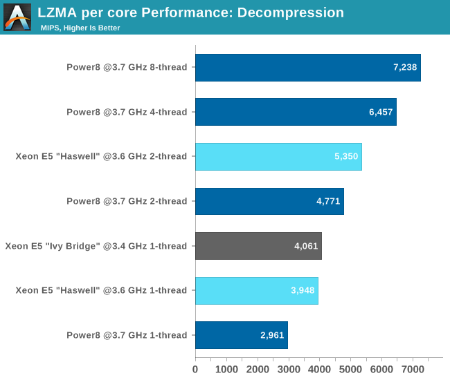
In Desktop workloads, it will probably reduce performance more often than not, but there definitely are use-cases where extra 2 threads will help. Just look at the scaling of Power 8 "Single Core" benchmarks vs Haswell from 1-4 threads(single core) 8 seams to be the real
61428dec.png


I also thought SMT-4 is rather unlikely on Zen3, but it certainly wouldn't hurt in some server workloads, if they cannot add more cores (just look at the scaling for SMT-2, there was a similar discussion ongoing, before it was released).
 

jpiniero

Lifer
Oct 1, 2010
14,487
5,155
136
POWER8 explicitly exists to game per-C licensing.
It would just have more cores if it didn't have to do that.

You would think software companies that do per-core licensing would be on to this, and charge more based upon the processor.
 

NTMBK

Lifer
Nov 14, 2011
10,208
4,939
136
Unified L3 is just cache minimizing bottle necks, nothing more. If AMD declared same IPC improvement as Zen 2, they have to do it via stronger back-end execution units.

SMT4 would reduce IPC, not increase it. Increased resource contention means that each thread will have lower performance.

And back-end isn't the only way you can get dramatic IPC improvements! Bigger re-order buffer, smarter branch predictor, improved prefetch, bigger uOp cache, etc.
 
  • Like
Reactions: Thunder 57

Ajay

Lifer
Jan 8, 2001
15,332
7,792
136
This is covered in the Q&A i posted, each core can write or read 32 bytes a cycle to the L3 cache (which ever way it hashes). each slice of the L3 has a buffer ( so multiple core can write to the same L3 slice each cycle). it is unclear if each slice can read and write 32 bytes a cycle or just read or write 32 bytes a cycle.
Clark really didn’t want to fork over more info did he. The L3 buffer or queue seems so obvious now (I thought some sort of arbitration or time slicing was going on). This also gives insight into how a single or double ported unified cache would work - larger buffers. Although, with 8 cores, there would seem to be allot of back pressure. Again, AMD has a lot of people who are smarter than me who worked on Milan.
 

Vattila

Senior member
Oct 22, 2004
799
1,351
136
I think the image showing “6 links” is an inaccurate oversimplification. […] You do not have 4 slices that need to be connected together, you have 8 things that need to be connected together, 4 cores and 4 cache slices. [...] I expect that it is 4 sets of read and write wires going from each core to each cache slice.

Sounds like you are in Tuna-Fish's camp — with a "slice-aware" L2.

Zen L3 Interconnect.png

I am in the second camp. I presume that slice-awareness is handled in the L3. It is simpler, and it correlates with AMD's slides.
 
Last edited:
  • Like
Reactions: DarthKyrie and Ajay

maddie

Diamond Member
Jul 18, 2010
4,717
4,615
136
SMT4 would reduce IPC, not increase it. Increased resource contention means that each thread will have lower performance.

And back-end isn't the only way you can get dramatic IPC improvements! Bigger re-order buffer, smarter branch predictor, improved prefetch, bigger uOp cache, etc.
I think you mean reduced single thread performance not reduced IPC.
 
  • Like
Reactions: DarthKyrie

JoeRambo

Golden Member
Jun 13, 2013
1,814
2,105
136
It is unclear how large of a chunk is interleaved between caches. Byte interleave seems too small. Perhaps a 32 byte cache line is interleaved across the 4 slices. They have shown slides with 32 bytes a cycle. That would be 8 bytes/64-bits from each cache slice. It is also unclear what you think a “link” is.

That is not how things work with caches. x86 standardized on 64 byte cache lines and common sense strategy is to use lower address bits as a selector to cache slice that is supposed to hold said cache line. There is no "interleaving" going on, as unit that is coherency etc tracked is cache line, so a slice either has (full) cache line for said address lower bits or it does not (and request goes to mem). You then transfer said cache line in as many cycles as your link width allows for to where it is needed.

With ZEN "coherency" domain is 4 core sized CCX that consists of cores+L1+L2 and L3 + tags (but not data) that hold what cache lines are inside the cores.

ZEN3 expands this coherency domain to 8 cores, but there is nothing there forcing AMD to keep same arrangement of 1 per core L3 slice, they can use for example 4 slices, while keeping tag part of coherency domain next to core.
Latency is going to rise anyway due to physical constraints, but 32+MB is what is needed for 8 cores as potent as Zen2.
 
  • Like
Reactions: Vattila

Gideon

Golden Member
Nov 27, 2007
1,598
3,520
136
I think you mean reduced single thread performance not reduced IPC.
Yes it would, but it probably wouldn't matter as much, as this feature could be disabled on non-server cores.

Speaking of which, I really hope that on top of the shared L3, Zen 3 finally makes the micro-op cache competitively shared, instead of statically partitioned.

I'm pretty sure Ivy Bridge did something similar (compared to Sandy Bridge) and it attributed to a nice performance gain, when no SMT threads were in use.

Here is how the Zen front-end is shared between SMT threads (which still seems to be the case with Zen 2, as it was mentioned in the newest developers guide) source:

Screenshot 2019-10-07 at 15.49.14.png
 

Vattila

Senior member
Oct 22, 2004
799
1,351
136
Speaking of which, I really hope that on top of the shared L3, Zen 3 finally makes the micro-op cache competitively shared, instead of statically partitioned.

This is something I have been thinking about: How static are statically partitioned resources?

What happens to a statically partitioned resource when you turn off SMT in the BIOS? Is all of the resource then available to a single thread executing on the core? Or does the thread still get only the same static partition?

If turning SMT off in BIOS opens up the whole resource to a thread, could this be configured dynamically by the OS? In other words, could the OS dynamically configure the core to partition resources (for SMT) or not (for single-thread)? Is this already the case, maybe?
 
Last edited:
  • Like
Reactions: amd6502

Ajay

Lifer
Jan 8, 2001
15,332
7,792
136
Sounds like you are in Tuna-Fish's camp — with a "slice-aware" L2.

View attachment 11690

I am in the second camp. I presume that slice-awareness is handled in the L3. It is simpler, and it correlates with AMD's slides.
Yes. And, why use 16 links when 6 links provide a fully meshed (all to all) connection. L2CTL's connect to the closest L3CTL, which can then propagate the L2 data to the correct cache slice. This probably means that the L3 interconnects are actually 32 bytes (so even more wires!). So in that bottom diagram, all the connections involve the L2CLT and L3CTL as physical connection point, as far as I can make out.
 
  • Like
Reactions: Kirito and Vattila

Vattila

Senior member
Oct 22, 2004
799
1,351
136
Yes. And, why use 16 links when 6 links provide a fully meshed (all to all) connection. L2CTL's connect to the closest L3CTL, which can then propagate the L2 data to the correct cache slice. This probably means that the L3 interconnects are actually 32 bytes (so even more wires!). So in that bottom diagram, all the connections involve the L2CLT and L3CTL as physical connection point, as far as I can make out.

Makes sense. With this solution, all the slicing logic and routing is fully encapsulated within the L3. And with just 4 additional links you can link up two 4-core CCXs into a 8-core super-CCX, as confirmed for Zen 3. Whether AMD will use this topology or something else, I don't know, but it seems like a simple extension and hence a plausible choice.

Zen 3 L3 Interconnect.png
 
  • Like
Reactions: Kirito

amd6502

Senior member
Apr 21, 2017
971
360
136
I wish they'd have left the presentation video up. It looks like we can expect modest IPC improvements. I think most likely a doubled L2 and maybe also bigger L1, and an additional ALU (5ALU+3AGU).

Speculation on greater than SMT2 ability isn't totally dead, it's just gotten much more unlikely. I'm in the Nosta and swordsman camp and think it's quite possible they would launch a n-way multithread early stage feature through an optionally enable feature that would be aimed more at beta tester and enthusiasts until the software ecosystem matures to the point where its use would be very optimal to the majority of the consumers.

In the linux kernel we are lately seeing a lot of new features to support heterogenous processing (though it's possible it's aimed for non x86 users) and prioritized and underprioritized tasks, resource contention prioritization/awareness and energy awareness,
 

Thunder 57

Platinum Member
Aug 19, 2007
2,640
3,697
136
Does anybody believe that AMD would release SMT4 feature on that presentation? Normally AMD is keeping new features top secret until final release of prouduct. New features and full specs was disclosed at special presentations to that particular core. They did that with Zen 1 and Zen 2. Why AMD would disclose one of the Zen 3 top secret feature on presentation of Zen 2 one year ahead? That does not make sense.

BTW. Technically AMD is not lying by specifying SMT2 for SMT4 CPU ;)...

...Speculation on greater than SMT2 ability isn't totally dead, it's just gotten much more unlikely. I'm in the Nosta and swordsman camp and think it's quite possible they would launch a n-way multithread early stage feature through an optionally enable feature that would be aimed more at beta tester and enthusiasts until the software ecosystem matures to the point where its use would be very optimal to the majority of the consumers.

In the linux kernel we are lately seeing a lot of new features to support heterogenous processing (though it's possible it's aimed for non x86 users) and prioritized and underprioritized tasks, resource contention prioritization/awareness and energy awareness,

Put a fork in it, SMT4 is dead. It was never a thing. There was never any evidence to suggest it.
 
  • Like
Reactions: NTMBK

amd6502

Senior member
Apr 21, 2017
971
360
136
Put a fork in it, SMT4 is dead. It was never a thing. There was never any evidence to suggest it.

when the fat lady sings.

It's basically a matter of time (Zen 4 surely should have 4-way imho) and a question whether they do SMT4 or general 4-way MT.
 

NostaSeronx

Diamond Member
Sep 18, 2011
3,683
1,218
136
Put a fork in it, SMT4 is dead. It was never a thing. There was never any evidence to suggest it.
SMT4 isn't dead, also there might be a CPU ACE unit to decouple OS threads from HW threads.

New patents coming up show cores executing more than 4-threads. (Four threads in execution, and many more in a micro-context buffer. In which, the L3 cache contains even more context info)

The SMT4 mode in Milan(256 macro-context unit)/Vermeer(64 macro-context unit) might need a new operating system. However, its SMT2 mode is backwards compatible. It might also have been delayed like NGG, ¯\_(ツ)_/¯.

Not 100% sure, but "full/heavyweight" context switches retain their security but can now occur in nanoseconds rather than in microseconds.
 
Last edited:

H T C

Senior member
Nov 7, 2018
549
395
136
Makes sense. With this solution, all the slicing logic and routing is fully encapsulated within the L3. And with just 4 additional links you can link up two 4-core CCXs into a 8-core super-CCX, as confirmed for Zen 3. Whether AMD will use this topology or something else, I don't know, but it seems like a simple extension and hence a plausible choice.

View attachment 11699

What if Zen 3 has an interposer? How would that change number of links?
 
  • Like
Reactions: Vattila